It may be a slight mismatch of the input JFETs due to specific matching conditions.
The 2SJ74 is pretty insensitive to Vds, but the 2SK170 is.
You can try changing R3t to see how that affects the input offset.
Is the offset positive or negative ?
Patrick
The 2SJ74 is pretty insensitive to Vds, but the 2SK170 is.
You can try changing R3t to see how that affects the input offset.
Is the offset positive or negative ?
Patrick
Thank you both.
The input offset is negative/-8mV.
I got 10 Q3s and Q4s. I don't know if it means much, but a multitester showed Vt=1.8V for the ZVN3306A and Vt=2.1V for most of the ZVP4424A. So by this measure, if it means anything, the pairs are off by 0.3V but this is the same for both boards.
Cheers,
Soren
The input offset is negative/-8mV.
I got 10 Q3s and Q4s. I don't know if it means much, but a multitester showed Vt=1.8V for the ZVN3306A and Vt=2.1V for most of the ZVP4424A. So by this measure, if it means anything, the pairs are off by 0.3V but this is the same for both boards.
Cheers,
Soren
I reflowed and checked the joints on the board with input offset, but it made no difference.
It seems peculiar that the voltage across R3t/4t is 33mV on the board with input offset and 11mV on the one that has not input offset. Similarly, the voltage across R52/62 is 0.56V different between the two boards.
It seems peculiar that the voltage across R3t/4t is 33mV on the board with input offset and 11mV on the one that has not input offset. Similarly, the voltage across R52/62 is 0.56V different between the two boards.
You can easily calculate the current through R3t/R4t, which should be 3mA minimum.
Increasing R3t should increase the current through Q1, which in turn should increase input DC voltage.
The difference between the two boards are a result of tolerance in the CRD current.
If you want them to be identical, you need to match the CRD current as well.
Patrick
Increasing R3t should increase the current through Q1, which in turn should increase input DC voltage.
The difference between the two boards are a result of tolerance in the CRD current.
If you want them to be identical, you need to match the CRD current as well.
Patrick
Thanks Patrick. The current through R3t/R4t seems too low on both boards: ~0.59mA on the board without input offset and ~1.65mA on the other with input offset. I can try increasing the values of these and measure the effect.
Is there any reason to play with the r1-4 divider and would this help getting Q1/2 closer to 7.5V?
Is there any reason to play with the r1-4 divider and would this help getting Q1/2 closer to 7.5V?

With some morning coffee in the system, I noticed your reference to the CRD. Measuring voltages across R58 on the two boards indicates the 'offset' board's CRD is 4.34mA and the other board has a CRD with 3.78mA. It seems I should start by using better matched CRDs and only then begin adjusting resistors. It will take a couple of days to get a selection of CRDs for matching.
Thanks Patrick. Would that mean increasing R52/R62 values by some 15% or so, to counter the 15% higher current of the CRD on that board?
Currently, R52/R62 have ~10.4mA on the wonky board. On the other board these have about 9mA.
I vaguely recall seeing a note about the R51/61:R52/R62 ratio, but can't seem to find it.
Currently, R52/R62 have ~10.4mA on the wonky board. On the other board these have about 9mA.
I vaguely recall seeing a note about the R51/61:R52/R62 ratio, but can't seem to find it.
I have been reading and tinkering with the board that has 8mV DC offset on the input. First, I was able to increase the current across R52/62 and R3t/R4t, by reducing the R52/62 values in steps. However, I could not get the Q1/Q2 drain voltages above 7.05/7.15.
At the moment, with R51/61 at 1000R and R52/62 at 275R, there is 15.3mA on R52/R62, 6.2mA on R3t/R4t, and Q1/Q2 at 6.92V/7.13V. The input offset remains 8mV. Increasing R3t to 33R moved Q1 to 7.01V. Going much lower for R52/62 value resulted in malfunction.
It is possible that I should just use this board with the input offset and the specs listed above. Alternatively, maybe I am missing something obvious...which is entirely possible given I am a beginner. I have had fun chatting with AI and swapping resistors, but seem to be missing something.
Any suggestions would be welcomed 🙂
Cheers, Soren
I assume you are using this with DAC output current of 1mA or 2 mA.
In that case, there is no need to have 6mA going through R3t,4t.
3~4mA would be sufficient.
To get the drain of Q1,2 up to 7.5V from 7V, you will need to have much larger values of R3t,4t.
Alternatively, you can adjust the ratios of R1/R3 and R2/R4, while keeping their sum more or less constant.
The input offset is largely due to mismatch of the JFET Idss, in the order of 0.2mA.
If you want to have it zero, you will either have to add a small resistor to the source of the J74 to effectively reduce its current, or change to a new pair of JFETs.
Patrick
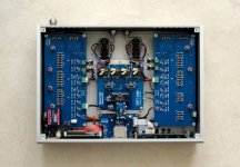
I have been enjoying the FC Cen for past few weeks and it is a wonderful IV stage. I think it deserves a PSU for each board/channel, so this is likely next.
The BOM specifies general purpose C3/4 caps. Would there be any benefit to swapping these with FMs/FCs/FRs, and/or adding a small bypass film caps to these two caps?
The BOM specifies general purpose C3/4 caps. Would there be any benefit to swapping these with FMs/FCs/FRs, and/or adding a small bypass film caps to these two caps?
- Home
- Source & Line
- Digital Line Level
- Folded Cascode CEN IV with fixed Rails