Pretty sure the Rg resistors have the wrong part number on the documentation. The called out part is a 0306 size part in inches. So small a pair of needle tweezers can't hold them and barely long enough to bridge the pads. The zero ohm jumpers are 0603 size parts in inches and fit the pads correctly. The part number for the the corresponding Susumu part in the correct size is: 754-RG1608P-221-BT5 from Mouser.
Here is a picture of the part from the documentation beside the zero ohm jumpers in the correct size.

FYI, check the MOSFET's, Q3 and Q4 before installing them, the writing on the MOSFET's go opposite the flat on the outline.
I should let Fran answer, since he put together the BoM with Mouser numbers from his own build.
He has been busy, so please bear with us.
Patrick
He has been busy, so please bear with us.
Patrick
The orientation of the MOSFET is correct as far as I can tell.
And I am pretty sure you have the right version of the PCB.
See picture attached from my working prototype.
Please make sure the PMOS is at the positive side and NMOS the negative.

Patrick
And I am pretty sure you have the right version of the PCB.
See picture attached from my working prototype.
Please make sure the PMOS is at the positive side and NMOS the negative.
Patrick
Hard to see in your picture. If you look strictly at the shape of the transistor, the outline is correct. But, Zetex puts the label on the small side. Very easy to get them turned around. Most people starting out think the flat side on the outline goes to the label. Here is a picture. I do have them in the correct positions.

This is something I had to look up, and then double checked - the "front" of the zetex mosfets are the curved side, ie the opposite of most transistors. Something to watch out for indeed. @RickRay - your orientation in the photo is correct, flat side matching the flat side on the PCB.
I'm sorry about the 0603 - I thought I had corrected that in the BoM, my apologies. I actually ordered those myself and saw the issue, so I should have had that corrected.
I'm sorry about the 0603 - I thought I had corrected that in the BoM, my apologies. I actually ordered those myself and saw the issue, so I should have had that corrected.
Last edited:

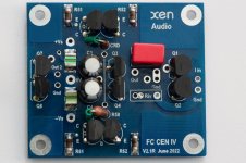
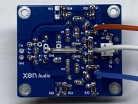
Is there a posted schematic that includes all the components on the CEN I/V board? Specifically R53, 54, 55, R63, 64, 65?
No, but they are very easy to trace on the PCB.
You can easily tell which other resistors are connected to them in parallel.
Patrick
You can easily tell which other resistors are connected to them in parallel.
Patrick
All of those are the bottom, opposite side of board, SMD MELF resistors.Is there a posted schematic that includes all the components on the CEN I/V board? Specifically R53, 54, 55, R63, 64, 65?
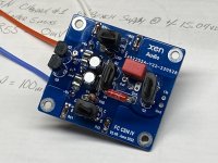
Drama free power-up of CEN I/V board, vital stats for channel#1
Bench supply adjusted to +/-15V
DC offset at initial power up: 100mV,
then quickly decended and stabilized @ -14mV.
Adding a 430K resistor to R55 nulled offset, 0mV.
Pos and Neg rails each draw 25mA.
Q3 Vgs = 1.728V
Q4 Vgs = 1.847V
R3t = 33R
R1~R4 = original BOM values
Bench supply adjusted to +/-15V
DC offset at initial power up: 100mV,
then quickly decended and stabilized @ -14mV.
Adding a 430K resistor to R55 nulled offset, 0mV.
Pos and Neg rails each draw 25mA.
Q3 Vgs = 1.728V
Q4 Vgs = 1.847V
R3t = 33R
R1~R4 = original BOM values
Attachments
You should measure Vs of Q3,4 (or Vd of Q1,2) relative to Gnd, not Vgs.
They should be about 7~7.5V.
And you trim that difference.
You can test the IV circuit on its own using a functions generator and a 2k resistor to simulate the DAC.
Then you know for sure it is working before connecting to anything else.
And make sure you remove the Riv and Civ on your original opamp IV before connecting.
Patrick
Last edited:
If you are using 10.5mA Idss for both Q1,2 and Q7,8, 25mA total consumption is too low.
The CRD already takes 4.5mA, R1~4 0.5mA, Q1,2 ans Q7,8 10.5mA each.
Nothing is left for Q3,4, which should see 3mA minimum.
I already mentioned earlier how you can increase the current through the current mirror (R52,62).
Patrick
The CRD already takes 4.5mA, R1~4 0.5mA, Q1,2 ans Q7,8 10.5mA each.
Nothing is left for Q3,4, which should see 3mA minimum.
I already mentioned earlier how you can increase the current through the current mirror (R52,62).
Patrick
- Home
- Source & Line
- Digital Line Level
- Folded Cascode CEN IV with fixed Rails