Scott, would you please describe what "bootstrapping the capsule" really means - what happens?
//
//
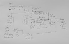
Scott uses nearly unity gain positive feedback to make the FET inside the capsule work at a nearly constant source current and a nearly constant drain-source voltage. That largely eliminates the distortion of the FET; the curvatures of its characteristics cause no distortion when it always works in the same point on the curves.
The NPN emitter follower copies the signal on the source to the drain to keep the drain-source voltage constant. The PNP does the same with the voltage across the source resistor, thereby keeping the source current nearly constant.
My latest sketch does the same in a more conventional, brute-force manner when you include the electrolytic capacitors from the op-amp voltage follower to the drain and to a midpoint of the source resistor.
Last edited:
@TNT Ah yes, I see.
If I were doing it (but I'm not) my first attempt would likely be to get the capsule powered up and connected to the inputs of the eval board in some manner, no matter if with caps or transformers or whatever. Then make some recordings and look at where the levels fall.
I suspect that the levels will be very low, with the bottom lost in the noise of the ADC. But at least it will let you know that it all works and will give you an idea of real world levels. Finding how far below 0dBFS the peaks are should be easy in your DAW. After that - modify!! 😀
Thanks Marcel - I think I can digest most of that. I would be interested to try to define a BOM for your circuit. I will probably also want to build fig10 for comparison.
Pano - it will most probably fold out as you say - I'm often very eager to get something going and defining a BOM and build a stage as the ones above will take some time 😉 - I agree on trying out the levels is a very good idea.
//
Pano - it will most probably fold out as you say - I'm often very eager to get something going and defining a BOM and build a stage as the ones above will take some time 😉 - I agree on trying out the levels is a very good idea.
//
Re: noise... how to asess these 2 charts..
LT1677 vs. OPA2156
//
Basically they are about equally good.
The LT1677 obviously has far less 1/f voltage noise than the OPA2156, but when you take into account psychoacoustic weighting curves like A- or ITU-R 468 weighting, you see that the gradual increase in noise density below 1 kHz actually doesn't matter much.
The LT1677's noise gets worse when the input voltage is very close to the rails, like when you record an extremely loud sound. That's because its rail-to-rail input stage consists of an NPN differential pair and a PNP differential pair. Very close to the rails, one of the two runs out of voltage headroom and the other has to work all on its own. Normally the noise of the stages partly averages out, but not when only one is active.
Like all bipolar op-amps, the LT1677 has a far greater equivalent input noise current than a JFET input op-amp or a CMOS op-amp. That would matter a lot if the source impedance were high, like if you would want to connect the op-amp straight to a condenser microphone without built-in FET. After the FET, the impedance level is so low that it doesn't matter anymore.
It's a very good choice. By the way, as you have +/- 15 V supplies available (the evaluation board requires those), a non-rail-to-rail op-amp supplied from the +/- 15 V should also work.
Regarding the diode stack in the picture from post #113, the idea is to stack LEDs and diodes until you have a voltage close to the DC bias voltage at the source of the JFET. You can add an RC filter between the stack and the op-amp to filter off any noise.
Regarding the diode stack in the picture from post #113, the idea is to stack LEDs and diodes until you have a voltage close to the DC bias voltage at the source of the JFET. You can add an RC filter between the stack and the op-amp to filter off any noise.
I'll take a static noise floor any day over a noise following the signal. Which parameter would indicate this aspect?
Maybe also:
OPA1692: https://www.ti.com/lit/ds/symlink/o...09704&ref_url=https%3A%2F%2Fwww.google.com%2F
OPA1612: https://www.ti.com/lit/ds/symlink/o...tps%3A%2F%2Fwww.ti.com%2Fproduct%2FOPA1612-Q1
OPA1656: https://www.ti.com/lit/ds/symlink/o...ww.ti.com%2Faudio-ic%2Ffeatured-products.html
So many choices.. distorsion or noise...
//
Do you want a single-ended supply for the mic board, as drawn in post #120, or is a symmetrical supply also acceptable?
Then the rail-to-rail requirement doesn't apply and you can just look for the op-amp that has the lowest noise at the 600 ohm output impedance of the source follower of the EM273, that is, minimal e_n^2 + (600 ohm*i_n)^2, and is able to deliver > 10 mA output current. You have to keep in mind that the former Linear Technology op-amps with base current compensation usually have misleading i_n values in their datasheets (only valid when the impedances driving the positive and negative op-amp inputs are equal, which they never are in any normal application).
It will probably become an OPA1612 or an AD797 then. An AD797 will be slightly worse than an OPA1612 because of the noise of the 100 ohm feedback resistor that it needs for stability when used as a voltage follower, but in fact both have completely negligible noise compared to the capsule.
It will probably become an OPA1612 or an AD797 then. An AD797 will be slightly worse than an OPA1612 because of the noise of the 100 ohm feedback resistor that it needs for stability when used as a voltage follower, but in fact both have completely negligible noise compared to the capsule.
Thanks Marcel!
Is this hardwire- or vero-bardable or should one go for a 2 layer PCB do you think?
The 8V (?) stab would one of the new super low noise ones (LT3045 etc) be of benefit? (Size?)
The diode array - 0,7V are quite large steps?
Your optional bootstrap... are you hesitating of its virtues... or? 🙂
//
Is this hardwire- or vero-bardable or should one go for a 2 layer PCB do you think?
The 8V (?) stab would one of the new super low noise ones (LT3045 etc) be of benefit? (Size?)
The diode array - 0,7V are quite large steps?
Your optional bootstrap... are you hesitating of its virtues... or? 🙂
//
When you use the SOIC-8 package version of the OPA1612 and solder some short wires to it, it should be Veroboardable. As the circuit is neither tried nor tested, Veroboard will give you the most options to change things if needed. To prevent hum, you will need a shielded enclosure around the Veroboard and some distance to the nearest mains transformer.
The noise of the regulator is filtered off by the 4.99 kohm resistor and 47 uF electrolytic capacitor (to ground or to the op-amp output, depending on whether you want bootstrapping). I expect that will suppress it sufficiently so you don't need an LT3042 or LT3045.
Regarding the diodes, you can try a red, green or yellow LED to make smaller steps. Red LEDs usually have the lowest and green the largest forward voltages, if I remember well. You could also replace the 1N4148 with one or more BAT85 Schottky diode(s) or play a bit with the current level, if needed. My best guess is a green LED and a normal silicon diode, as drawn.
Actually an alternative could be to choose the LED and diode such that you get about 2.3 V, replace the bottom 2.8 kohm resistor with 1 kohm in series with a 5 kohm trimming potmeter (wiper connected to the positive side) and trim it until the output voltages are about equal. That probably leads to a more reproducible source bias voltage than what I had in mind.
I'm pretty sure the bootstrap will reduce distortion like Scott's does, what I'm not sure about is whether it is acceptable to you. Even though they are not in the primary signal path and only reduce second-order effects, there are AC coupling capacitors in the bootstrapping circuit.
Cool. Yes, I did actually suspected that these capacitors must be seen as being on the signal path but ea a bit hesitant to ask this so to come out as ungreatful for the great support you give 🙂
I will arrange so that both options can be avaluated somehow.
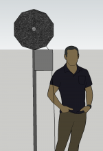
I have some ideas for housing the capsules that would give great shielding... see if I can draw something to test them here...
//
I will arrange so that both options can be avaluated somehow.
I have some ideas for housing the capsules that would give great shielding... see if I can draw something to test them here...
//
Ordered a set of two matched capsules from England which seem to be the only "safe" place to buy from. Mailed Primo Germany but no response. Payed Total of the transaction (taxes incl.) : £ 49.87 - interesting to see what extra cost will be added now that England is out of EU...
On to the electronics...
//
On to the electronics...
//
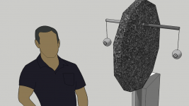
Recording rig Rev 0.
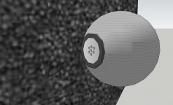
Reflections from the micbox....
//
Reflections from the micbox....
//
Attachments

Last edited:
Cool. Yes, I did actually suspected that these capacitors must be seen as being on the signal path but ea a bit hesitant to ask this so to come out as ungreatful for the great support you give 🙂
I don't subscribe to capacitor nonsense, the circuit as given won the European Triode Fest recording shootout against plenty of expensive tube mics and gear.
Good. Me neither really but I do strive for as clean signal path as absolutely possible. In this case leaving out the caps is a case of sub-optimisation i.e. gone to the length being contra productive.
//
//
Last edited:
- Home
- Source & Line
- Digital Line Level
- Fixed gain field recorder?