Thanks - I was quite happy with the result.
On an other "note"... how do one design a mic stand that can raise 2,5 meter (10 feet) above the floor that has the least:
- pick up from the floor
- pick up from the air
?
Gearspace.com - View Single Post - Mic Stand mass can affect sound?
//
On an other "note"... how do one design a mic stand that can raise 2,5 meter (10 feet) above the floor that has the least:
- pick up from the floor
- pick up from the air
?
Gearspace.com - View Single Post - Mic Stand mass can affect sound?
//
Sand bags on the stands? They would add weight and sand is excellent at damping sound. Kitty litter, too, but I think sand is better.

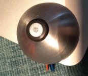
Some progress on the mic build... Maybe I want the capsule flush to the sphere. But these dimensions are small compared to 20k wave length... but still...
Wimas are 10uF... so 47 -> 10 and 100 -> 20 uF... 1Hz -> 5 Hz.... OK?
//
Wimas are 10uF... so 47 -> 10 and 100 -> 20 uF... 1Hz -> 5 Hz.... OK?
//
Attachments


Last edited:
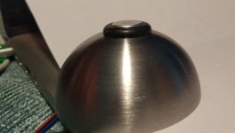
Try it and you'll hear. It is certainly better than the standard application of the microphone capsule.

Maybe flush, but then fill in the trough with modeling clay, or something else easy to work with.
Cheers
Cheers
Yes, thinking about it I think I will do it flush. The grommet was quite hard rubber... I'd like a more compliant isolation and I think I will make one out of silicone.
About cabling and ground/0 ref... there is 2 paths:
- to mic - power feed: +18, +18V / -18V and Ground
- from mic - signal returned: +out, -out and a Zero
Now, I'm thinking of running these as 2 separate shielded groups in one joined "cable". But do I run both Ground and Zero? Could this form a ground loop? If only should be used I'd go for the Zero as this is the fragile signal and the receivers of the power has high pssr / isolation... What do you think?
//
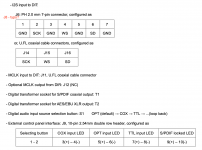
Can I use a Ian Canada SPDIF board for the i2s to toslink conversion?
I2S input
LVTTL (3.3V) logic input level
44.1 KHz, 48 KHz, 88.2 KHz, 96 KHz, 176.4 KHz, 192 KHz – 16- or 24- bit 7-pin PH 2.0mm connector
from: DocumentDownload/SPDIF_InterfaceBoard.pdf at master * iancanada/DocumentDownload * GitHub
//
I2S input
LVTTL (3.3V) logic input level
44.1 KHz, 48 KHz, 88.2 KHz, 96 KHz, 176.4 KHz, 192 KHz – 16- or 24- bit 7-pin PH 2.0mm connector
from: DocumentDownload/SPDIF_InterfaceBoard.pdf at master * iancanada/DocumentDownload * GitHub
//
Attachments

Regarding zero/ground: I think I'd also just connect the zero. If you do run ground and zero, keep them very close to each other to minimize the enclosed loop area.
Can I use a Ian Canada SPDIF board for the i2s to toslink conversion?
I2S input
LVTTL (3.3V) logic input level
44.1 KHz, 48 KHz, 88.2 KHz, 96 KHz, 176.4 KHz, 192 KHz – 16- or 24- bit 7-pin PH 2.0mm connector
from: DocumentDownload/SPDIF_InterfaceBoard.pdf at master * iancanada/DocumentDownload * GitHub
//
Yes, that should work when you loop through the MCKO from the PCM4222 evaluation module to the master clock input.
SCK: official Philips/NXP name for what's called BCK in Sony lingo
WS: LRCK in Sony lingo
SD: data
Last edited:
Are you thinking about the case with or without FPGA board?
For the case with an FPGA board, the FPGA board will be I2S master and will drive the I2S input of the Ian Canada board.
Besides the I2S signals, the Ian Canada board needs a master clock at J11. It has to be either 128 or 256 or 512 times the decimated sample rate. You could use J4 pin 13 of the PCM4222 evaluation module for that, as it carries a clock signal of 128 times 88.2 kHz or 128 times 96 kHz. J4 pin 13 then has to be connected to an input of the FPGA board (pin 5 of SV2, mck) as well as to J11 on the Ian Canada board.
The second FPGA board arrived safe and sound in Haarlem today. I'm going to keep it stored until you report a problem.
- Home
- Source & Line
- Digital Line Level
- Fixed gain field recorder?