Hi LC,
Thanks for the response. This is not the final home for the modules. This was a very quick proof of concept test to make sure everything worked before I put the extra effort to finalise the chassis.
I have done the same thing with every amp I have built and have never had an issue before.
The problem lay in the cabling I was using as the adapter cable sockets were loose on the cheap phono cable I was using to test. They worked loose as I moved the ipod and caused the amp to be effectively plugged in and out while running and probably not with both signal and ground at the same time. I thought the cable was loose at the ipod and only when I tested the other side did I realise that it was the phone cable that was loose.
Complete operator error and accident on my behalf.
I found this here Speaker Failure Analysis
"High frequency oscillation at full power IS damaging to amplifiers. Smoke will appear as resistors and capacitors in output Zobel networks burn up and BJT amps will quickly expire as transistors fail from excess dissipation. Amps using lateral MOSFETs will normally survive such events with only slight damage. The causes of such oscillation lie with operator error and bad cabling practices"
Pretty much what you said and exactly what I did.
I will check the values again but all seems OK for the short term. Does the resistance normally go up as they burn?
If I need to replace them can you give a link to the same or equivalent part used?
Thanks
Would these be OK to replace 39 Ohm Zobel Resistors?
http://http://au.element14.com/panasonic-electronic-components/erj12sf39r0u/resistor-thick-film-39ohm-1-2010/dp/2324413
Panasonic size 2010 0.75W thick film +- 1%
http://http://au.element14.com/panasonic-electronic-components/erj12sf39r0u/resistor-thick-film-39ohm-1-2010/dp/2324413
Panasonic size 2010 0.75W thick film +- 1%
Yes these are cool.Would these be OK to replace 39 Ohm Zobel Resistors?
http://http://au.element14.com/panasonic-electronic-components/erj12sf39r0u/resistor-thick-film-39ohm-1-2010/dp/2324413
Panasonic size 2010 0.75W thick film +- 1%

OK, input GND connection lost can cause HF burst, making zobel resistors dissipate more than expected normally, ending in smoke.
Just change all with burning marks to be on a safe side.
How come you choose only one SMPS to supply four modues? Mid-high speakers only?
Hi LC,
I understand now how and why it happened, just need to repair it!
I have been looking at hot air rework stations as this seems like the easiest way, I do have another use for one but have been trying to hold off getting any more tools.
Choice of single SMPS was down to cost and size. This amp will power one speaker, two channels for high and mid one for each bass driver. 80w per channel is the normal recommended power so this is still overkill.
Active systems are much kinder to amplifiers. In the previous generation I used lm4780 chip amps with linear supply and fairly minimal capacitance.
Even these could take it almost to x-max limits.
One quick advice regarding SMD-s, all burnt resistors meant to replace just simply broke them in half and clean them out with regular solder tip. New resistors can be soldered in a very easy way then, first solder one side to make an alignment and then both sides firmly. 😉
Thanks LC that sounds like a good idea. What is the best way to break them in half without causing any damage to the board?
Press them down with - screwdriver to PCB so the ceramic base will brake like glass. You'll see a fracture line in the middle of SMD's body, meaning it is spilited in half. Then is very simple to clear each half off the PCB with soldering iron tip, one half at a time.Thanks LC that sounds like a good idea. What is the best way to break them in half without causing any damage to the board?
Clear the excess solder tin from solder pads and solder new SMD resistors on their places. 😉
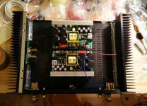
Very nice layout but be careful First One module is positioned wrong, power transistors have to be located at bottom side of the case, meaning +/- input pads to upper side of chassis, near the cover plate.I start building my first First One [emoji1]

The FO is just put inside for the picture!
But thank's I don't know the FO have up ans down
It is a matter of air movement(warm:up and cold:down),hence the heat producing parts (i.e. power transistors) must be located near the bottom of the heatsink for better cooling.
You didn't get User manual with the modules? 😕My FO is sounding for the first time, even with the lack of help 🙁
Anyway in this way you have learned more in longer terms.
You didn't get User manual with the modules? 😕
Anyway in this way you have learned more in longer terms.
No user manual, could you please send it to me?? jpcb@hotmail.com
Thanks
Hi Andrej,
One channel of my FO died. 😡 I checked the bias on TP1 - TP2 and TP3 - TP4 and 0mv reading. Even though I rotate the trimmer resistor on both sides, no change of reading on the meter. The DC offset reading on the output terminal is 1.12 V. Checked the output bias current and its only 20mA. No sign of burn components. I checked components by resistance reading comparing to the working channel and they measure almost the same. If its a burned Output tranny, then it suppose to show a different reading, correct? Any suggestion to fix it?
Would you mind to share the schematic to me thru email, so I can go stage by stage checking of components? Thanks.
Hi fredlock
Try to measure voltage drop on R15, R16, R17, of course with shorted +IN and -IN.
Are supply +/- voltages OK?
BR L.C.
Try to measure voltage drop on R15, R16, R17, of course with shorted +IN and -IN.
Are supply +/- voltages OK?
BR L.C.
Hi Theo
DC sense PCB-s are here, 96 pcs. available at the moment, will be produced more if any interest. 😎
They'll be sold as a small PCB kit, including:
- DC sense PCB, 1 pcs.
- optocoupler, 1 pcs.
The rest of the passive materials should be provided by the user, nothing special few resistors, diodes, capacitors.
DC sense PCB triggers the optocoupler at more than +/-1 V DC on the speaker output, which closes its output darlington to very low Uce_sat, thus close the circuit from shutdown pin to GND of any SMPS. Switch Imax=100 mA.
Price 8,00 EUR for one DC sense PCB kit. 🙂
GB starts bellow. 😉
Regards, L.C.
Assembling my F-O modules into an amp, I think I need a couple of the DC sense PCB kits. Still got some?
TIA!
Greg in Mississippi
Hi fredlock
Try to measure voltage drop on R15, R16, R17, of course with shorted +IN and -IN.
Are supply +/- voltages OK?
BR L.C.
I will try to do some measurement this weekend. I'm currently busy at work.
+/- voltages on the amp board was fine.
What voltages should I expect to measure on R15, R16 and R17? Could you give me some numbers? Thanks for your support.
Fred
Assembling my F-O modules into an amp, I think I need a couple of the DC sense PCB kits. Still got some?
TIA!
Greg in Mississippi
Yes, mail me a request. 😉
I will try to do some measurement this weekend. I'm currently busy at work.
+/- voltages on the amp board was fine.
What voltages should I expect to measure on R15, R16 and R17? Could you give me some numbers? Thanks for your support.
Fred
R15 - 1,4 V
R16, R17 - 33 V
LC, I got the chance to check the voltages today, as you recommended at R15, R16 and R17.
R15 = 1.03V R16 = 31.48V R17 =- 30.64V and has a DC Offset of 980mV
0V measurement on TP1-TP2 or TP3-TP4. I tried fiddling around TR1 and TR2 but no change.
The working channel measures, R15 = 1.13V R16 = 28.2V R17 = -31.87V and has a DC offset of 2mV.
TP3-TP4 = 150 mv
I think one of the transistor on the input pair had a problem. I checked it by resistance reading and compared with the working channel, there's some discrepancy.
It could have been easier to troubleshoot if I have a schematic. Following the PCB tracks is difficult because its small, double sided and crowded. What would you suggest this time? Thanks.
- Home
- Vendor's Bazaar
- First One - mosFET amplifier module