The amp is very simple.
Please measure voltages between gate of output transistor N and GND and repeat the same measurement for P type output transistor.
Please measure voltages between gate of output transistor N and GND and repeat the same measurement for P type output transistor.
Another PCB ver of BG1-BJT, ready to connect with PSU. Some pics:
An externally hosted image should be here but it was not working when we last tested it.
An externally hosted image should be here but it was not working when we last tested it.
An externally hosted image should be here but it was not working when we last tested it.
An externally hosted image should be here but it was not working when we last tested it.
An externally hosted image should be here but it was not working when we last tested it.
bc550c/560c
bd139-16/140-16
2sc4793/2sa1837
mjl3281/1302
In a few days I will try this amp, how works and how play music 🙂
Also, I'll do some measurements on the scope.
BR,
Boban
Boban, which version of schematic did you use?
The amp is very simple.
Please measure voltages between gate of output transistor N and GND and repeat the same measurement for P type output transistor.
Hi Borys
I managed to get the bias working correctly. I must have recieved a bad batch of IRF mosfets either that or I've subject them to fatal static charge or transient as around 5 of mosfets out of 20 are dead. Anyway thanks for your help much appreciated. I have it working now on the test bench. I will post some pics of the completed assembly soon.
Kind Regards
Dominic
OK, shortened the track lengths for C9/C10 and used SMD bypasses on the underside as suggested - however, size of C9/C10 had to be reduced from 16mm to 12.5mm to get the most placement benefit. That's probably OK, since there's enough choice of 470..1000uF, 50 to 63V caps in 12.5mm.
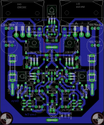
The overall dimensions are down to 2" x 2" (~50mm x 50 mm), which seems to be close to optimal for the layout, allowing interchangeable use of TO3P and TO247 outputs..
Hi linuxguru, Very nice compact design. Can you post the PDF file? Intersted on this.
Thank you.
Boyet
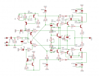

Boban, which version of schematic did you use?
Hi, this one:
An externally hosted image should be here but it was not working when we last tested it.
Sir Borys, cou1d you kind1y confirm if the posted BG1-BJT schematic was the 1atest update? I am current1y drafting a new pcb design. 🙂 Many thanks!
Beautifully designed PCB.
Please give the display rear side PCB in pdf.
thank you!
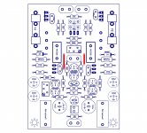
^here you go Radio, take note though, BD139 bias sensor must be mounted on the main heatsink via wire Iinks. VAS transistor are not designed to be mounted under the board either, but there's no stopping you of finding a means of doing it without damaging the pcb copper tracks. (bottom copper.pdf for toner transfer) 🙄 😉
Attachments
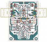
beautiful PCB for amplifier
Thank you Mr. Abetir for PCB.😉
I just have this question: What is the sound of this beautiful amplifier?
What is the bass and like that stuff?
best regards
cheers!
P.S.
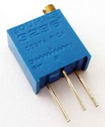
Here's what it looks like multi-turn potentiometer 1k (R18), so this should be put on the PCB-layer.
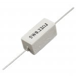
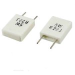
Resistor R1, R2=0R22/5W.
Thank you Mr. Abetir for PCB.😉
I just have this question: What is the sound of this beautiful amplifier?
What is the bass and like that stuff?
best regards
cheers!
P.S.
Here's what it looks like multi-turn potentiometer 1k (R18), so this should be put on the PCB-layer.
Resistor R1, R2=0R22/5W.
Attachments

Last edited:
^the footprints are modeled to these types (attached image), but you can also use those types as in your sample, make the rectangular white wirewound in vertical (upright) position.
hope it helps! 😉
OK!

Sir Borys, cou1d you kind1y confirm if the posted BG1-BJT schematic was the 1atest update? I am current1y drafting a new pcb design. 🙂 Many thanks!
C16 and C15 --> no need to solder them (they were ther in case any parasitic oscillations)
R19 can be lowered to 100-330 R value.
R4 and R5 --> you can replace them with 22R (in some cases 33R) resistors, next is the driver stage so vas doesnt have to be biassed so high (some heat issues)
Everything else is just fine.
Last edited:
C16 and C15 --> no need to solder them (they were ther in case any parasitic oscillations)
R19 can be lowered to 100-330 R value.
R4 and R5 --> you can replace them with 22R (in some cases 33R) resistors, next is the driver stage so vas doesnt have to be biassed so high (some heat issues)
Everything else is just fine.
Mr Borys, for which the schematic is working?🙄
thanks
VSSA BJT BG1 + Mr.Evil/PMI capa-multi PSU + uPC speaker protect
Not tested yet...
An externally hosted image should be here but it was not working when we last tested it.
Not tested yet...
Sir Borys, cou1d you kind1y confirm if the posted BG1-BJT schematic was the 1atest update? I am current1y drafting a new pcb design. 🙂 Many thanks!
Hi Abetir!
Why the difference in the values of the components between the schematic and the PCB? (see #665)😕🙁
thank you!
^Which values you are referring to? I only see the 22pf (pcb) instead of 33pf (schematic) cdom on VAS transistor and some changes on rail voltage smoothing caps value (not so critical). Some resistor values needs to be adjusted to suit your applied rail voltage. You need to build it first then apply Borys changes, the board should work fine. 🙂
Last edited:
Mr Abetir, this is changes in components?😕🙄
P.S.
Hole on components (resistors, capacitors and transistors BC...) on PCB for the drill 1mm no for 0.7mm?!
It will be alright!😉
thank you!
P.S.
Hole on components (resistors, capacitors and transistors BC...) on PCB for the drill 1mm no for 0.7mm?!
It will be alright!😉
thank you!
Attachments

Last edited:
i have some irfp260n hexfet mosfets.will a quasi complementary output work with this amplifier?if yes will there be any layout??
there are 2 nice layouts for one pair of output transistors 2sc5200/1sa1943. has anyone tested both?does one sounds better than the other ??
there are 2 nice layouts for one pair of output transistors 2sc5200/1sa1943. has anyone tested both?does one sounds better than the other ??
Attachments

- Home
- Amplifiers
- Solid State
- FET-hex explendit amplifier