F6 . if made correctly , can't be responsible for any bass deficiency in system
there is always possibility that 25W is not enough to make your ears happy , when combined with your speakers , but then it is not F6 as culprit , it is mismatch between speakers and amplification
for me - 180mm dia cones with 88db/1W/m sensitivity , married with 25W amp ...... isn't match made in heaven , if I'm expecting music bliss
if happy cruise is what's expected , then OK ( for several years I was happy with 15W amp and LS3/5 clones ) ....... I like and enjoy more efficient and more sensitive speakers , which mostly means they need to be bigger .....
Hello!
I have solved the problem with the basss🙂). I have removed the fuse from the circuit completely and also I have moved away all the supply wires from any ground path (wire ,base plate...).The sound is fantastic now! I like it a lot. Kudos are singing effortlessly and so so so so sweet !!! 🙂)
Now I`m thinking to add a buffer like B1 buffer with triode.I hope it will be a good matching.
Thanks a lot.
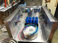
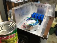
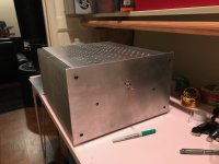
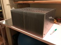
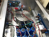
Chassis layout check before I drill lots of holes
Hello,
I am just to the point of drilling lots of holes in my chassis. I though it would be wise to check the layout with the fine minds on this forum, to minimize the number of times I fabricate chassis panels.
The heatsinks are about 5U tall and 400mm long The chassis is about 300mm wide on the interior. Since my chassis is a bit narrower than many, I thought it would be better to mount the soft start and DC protection board on the back panel, rather than on the bottom plate.
also as the chassis is narrower and my transformer (Antek 4218) is closer to my amp PCB's it would be a good idea to use a transformer cover. It turns out large food cans are just the right diameter for this transformer.
Attachments

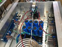
Finished my F6 build last night, really enjoying the sound!
Thank you diyaudio for providing a platform to share information and source parts, another thanks to Nelson Pass for sharing your creation, and another thanks to 6L6 for patiently answering so many of my questions throughout the build!
Thank you diyaudio for providing a platform to share information and source parts, another thanks to Nelson Pass for sharing your creation, and another thanks to 6L6 for patiently answering so many of my questions throughout the build!
trouble with one side of my F6
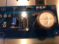
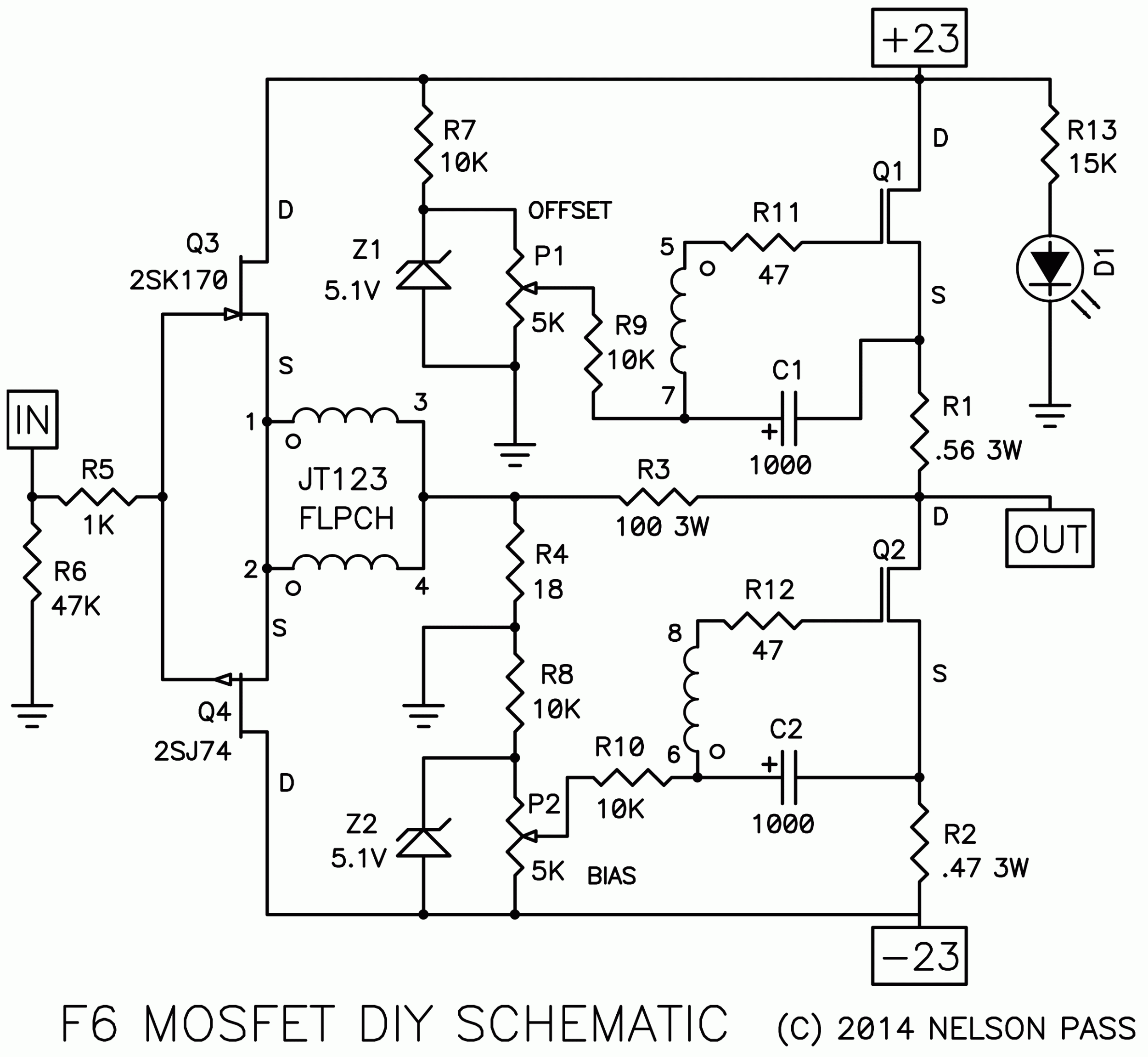
I have completed my PSU and F6 boards. The PSU checks out with 25v on both the + and – sides with no load. One side powers up fine, the LED lights and I am able to set Bias at 0.5v and set offset near .0v. The heatsinks warm up to around 100c, middle pins of Q1 and Q2 warm to around 130c.
The other sides’ LED does not light up and the board will not bias or set offset properly. I set the bias to around 0.5 v. I then set the offset to around 0v. Going back to the bias I find it now reads around 0v. Changing these makes them go back and forth. The bias and offset adjustments on this board seem to react more quickly than the board that works.
-I have checked the Zener diodes, LEDs and capacitors for polarity and all checks out.
-I have checked the LED by running 3v dc from 2 AA batteries in series across R13 and the PG pad with + attached to the far side of R13 and – attached to PG pad. The LED will light this way.
-I have checked the values of the resistors and found:
R1=.56r
R2=.47r
R3=100r
R4=18r
R5=1k
R6=47k
R7=2k
R8=2k
R9=10k
R10=10k
R11=110r
R12=110r
R13=15k
I reflowed all the solder joints and added a bit more solder to each joint. I have checked continuity across most of the easily accessible points and found no problems, and I believe the soldering is ok. I have measured resistance across:
v+ and out at 192r;
v-and out at 198r,
v+ and PG at 111r
v- and PG at 116r
These are similar values to the board that works.
v+ and out at 195r;
v-and out at 198r,
v+ and PG at 115r
v- and PG at 116r
I have not checked the function of the Zener diodes, capacitors, Pots, or transistors. At this point I am wondering if I have installed Q1 and Q2 in the wrong spots. I did not want to desolder to check as this may heat these up too much and damage them, unless knowledge folks felt that was a likely cause of the problems I am havng.
Any suggestions?
Attachments
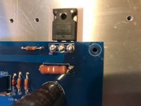
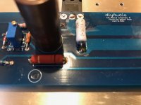
That was easier than I imagined. Didn’t think I would be able to read the tiny text with my awful eyesight. Q3 & Q4 are in the right place. The thermal grease really made the lettering pop. Needed a magnifying glass before I assembled them. Oddly I was hoping they were installed wrong.
I’m using the schematic from post #1 on this this build guide thread. I changed the zener diode to 5.1v and R7 & R8 from 10k to 2k. Also R11 & R12 were changed from 47r to 110r.
Is the LED only a power indicator?
Is the LED only a power indicator?
Last edited:
you certainly MUST have 5V1 across both zenners
though , if you're using IRFP outputs , change these 5V1 to 6V8
no problem with other changes
LED is just power On indicator
though , if you're using IRFP outputs , change these 5V1 to 6V8
no problem with other changes
LED is just power On indicator
a step forward
I checked my A channel board (the one that the LED would not light) several times for correct values. Next I checked diodes, and capacitors for function and found them to be ok. As it appeared that it would not be possible to check the transistors without unsoldering them, I then started to check continuity between adjacent components hoping to find a bad solder joint. During this process I discovered that my A channel board (and presumably all others) does not follow the schematic exactly. The LED and dimming resistor are connected from V- to ground rather than from V+ to ground as shown in the schematic. I reversed my LED and it now lights up.
With the LED working and much higher confidence about there being nothing wrong with the board I resumed testing it with the power supply and setting bias and offset. I discovered that the bias and offset do affect each other but with greater patience and confidence nothing was wrong, I managed to set bias and offset to 485mv and around 1mv respectively.
Now to wire the input and test with a signal and some cheap speakers.
Does anyone know if there is a reason the LED is wired differently on the two channels?
While checking the board was time consuming I think it was time well spent. I am a lot more familiar with the circuit, even though I still don't understand how it works very well.
ref to schm in first post, upper led is powered from upper rail and gnd, while lower LED is powered from GND and lower rail
pretty logical ...... LED needing to be situated on , well , same level as G-S of adjacent MOS/FET
pretty logical ...... LED needing to be situated on , well , same level as G-S of adjacent MOS/FET
Unfortunately, I dont follow the logic, I dont understand why the two channels would not be the same with respect to the LED coming from v+ on one side and v- on the other.
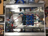
Fortunately, it's academic as my F6 project works and sounds great. I owe a heartfelt thank you to Nelson Pass for sharing his work with the DIY community and to DIYaudio for providing circuit boards and technical support by way of it's helpful members, especially 6L6, without the build guide I don't think I could have completed this successfully.
Yes, the inputs in some of the photos had not been connected, and the outputs are now wired to bypass the speaker protection board, which does not work, I will be trying the protection board a second time.
Attachments

Last edited:
Nice work there..
Curious re the Soup can as Tx shield.. Klever.
Does it actually do anything though ?
Curious re the Soup can as Tx shield.. Klever.
Does it actually do anything though ?

It's a large size tomatillo can. Totally different. 😉
Does it do anything? Not sure, it has a pretty low impedance connection to ground so it may work. I found a thread regarding transfomer sheilding, thin steel was one of the recommendations. The can is pretty thin steel. I'd have to do a listening test, I'd be surprised if it really makes an audible difference. A lot of folks seem to use the same transformer (antek AS 4218) and don't ever feel a need to use a transformer shield. It was easier to fabricate an install now rather than later. It cost very little, and I enjoyed a delicious pot of chili verde as a bonus. The can just was the perfect diameter.
Belt and Suspenders.
- Home
- Amplifiers
- Pass Labs
- F6 Illustrated Build Guide