The green LED biasing mod was very helpful for an F6 that was running at higher voltage and bias current. Difference is between needing more than an hour to reach final bias points for current and offset vs about half an hour. I was using an LM329 reference before the LEDs.
That same F6 (mine) was also using FQH44N10 output devices, which sounded better with the higher operating voltage and current. I built a special input stage to handle the higher voltage, so this mod is maybe not for everyone. I mentioned this amp recently in the Sony VFET builders thread.
That same F6 (mine) was also using FQH44N10 output devices, which sounded better with the higher operating voltage and current. I built a special input stage to handle the higher voltage, so this mod is maybe not for everyone. I mentioned this amp recently in the Sony VFET builders thread.
Last edited:

That same F6 (mine) was also using FQH44N10 output devices, which sounded better with the higher operating voltage and current. I built a special input stage to handle the higher voltage, so this mod is maybe not for everyone. I mentioned this amp recently in the Sony VFET builders thread.
Tungsten,
I looked through some of the other threads and all I got was that you used a modified diamond buffer inspired by MJ's Austin board in the M2x along with the FQ44N10 output MOSFETs. I also understand that you used dual 300VA doughnuts along with dual SLB supplies - that part is easy.
Do you mind showing pics, posting the schematic, etc...of that modified input board for the rest of us who want to experiment? 😀
Thanking you,
Anand.
I built my F6 front end cards on Veroboard, aka strip board. I don't have a schematic, as I got used to reading the strip layout as such. It mainly substitutes Toshiba TTC004B and TTA004B for the output devices. I also used 10 Ohm base stopper and emitter degeneration resistors instead of the RC network across the bases of the output devices. Works quite well.
I tweaked the SLB components a little to use lower VceSat bipolar transistors, and got good stability in the CFP. Here is a list of the changes that were made to the SLB, referenced to the SLB-APRIL-11-2019 schematic:
R1, R2: 18 Ohm
C7, C8, C13, C14: SLPX183M050H9P3 (18,000 uF, 50V)
Q9, Q11: KSC2690AYSTU, KSA1220AYS
Q10, Q12: MJW1302AG, MJW3281A
R17, R18: 1.8 Ohm
The transformers I used were the Antek AS-3222, which gave me +/– 26V power rails with 1.85A bias current.
Attachments
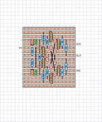
I built my F6 front end cards on Veroboard, aka strip board. I don't have a schematic, as I got used to reading the strip layout as such. It mainly substitutes Toshiba TTC004B and TTA004B for the output devices. I also used 10 Ohm base stopper and emitter degeneration resistors instead of the RC network across the bases of the output devices. Works quite well.
Tungsten,
Thanks. I am comparing and contrasting Mark's Austin schematic to what you have shown me. It also looks like you omitted the output 220uf capacitor (C1) and also a small bypass cap (2.2uf) across the V+ rail. R8 and C4, the RC network across the bases of the output devices were omitted as well. IC1 and IC3 are 10V voltage references, and I take it that you used an LM4040?
Very nice! Is the omitting the 220uf/C1 output capacitor okay as long as we don't have any dc on the input of the amplifier? I am asking since there is the Jensen input phase splitter transformer.
Thank you for sharing your experiments. The Verocard is a cool idea and now that I think about it, one can design a multitude of input buffer/small gain cards for the F6 as long as it has a low output impedance as Nelson recommends in his F6 article from 2012. Heck, I am surprised that the M2 morphed into an M2x platform but the F6 didn't. And the F6 even has options for the output MOSFETS where you can use Semisouth R100's. The F6x platform? Hmmm...something to think about.
Best,
Anand.
Last edited:
Yes, your summary of the changes is accurate. I used LM4040-10 for the references; they are depicted as diodes in the strip board diagram. The R8 & C4 network was intended to control something called "minority carrier injection," a somewhat rare phenomenon that may or may not affect the larger Toshiba output devices used here. Mark J. was no doubt following due diligence in the original design.
There is certainly a question of whether and where to install DC blocking caps in the front end. Before the buffer? Before the transformer? Mine is doing Ok without, but there are certainly scenarios where a DC blocking cap could alleviate issues. I'm unsure of the impedance present at the input to the Jensen transformer. Any DC blocking cap needs to take this into account.
I have considered doing an F6 PCB layout that either incorporates the diamond buffer or even allows for swapping alternate front ends. That might be the project that I use to learn KiCad. Other project are keeping me busy for now.
Sign me up if you go for it.
As to the input impedance facing the Jensen transformer, I recall Pass saying in his 2012 article that the input impedance of the Jensen trafo is 20k ohms (at low frequencies). He also said, taking into the account the input capacitance of the Jensen transformer, that a preamp with an output Z of 100 ohms or less will work best and that 600 ohms or more will make the F6 have a real soft top end. So a low source impedance is ideal. That isn't a problem in my world since I use digital, mostly solid state and if I were to use tubes, it would be something with current capability!
Page 6 of his article.
On Page 5, the unbuffered F6 is shown and that can be base for all sorts of experimentation with tons of daughter board potentials. The overall gain of the amp is only 14dB. Lots of room to play for both buffered cards and gain cards.
Best,
Anand.
Last edited:
Regarding the power supply,
It looks like there’s 2 different versions. The older one using jfet’s uses the heatsinks on the psb and the mosfet version which eliminates the need for those heatsinks. Is that correct?
If so that portion of the power supply board can be removed?
It looks like there’s 2 different versions. The older one using jfet’s uses the heatsinks on the psb and the mosfet version which eliminates the need for those heatsinks. Is that correct?
If so that portion of the power supply board can be removed?
What power supply? What schematic? What boards? What do you mean by "old" or "new"? What are you referencing? I don't know of one that uses JFETs, but that doesn't mean one does not exist.
Links or detailed description, please.
Links or detailed description, please.
Can someone tell me the minimum wire gauge that can be used for the F6 build? I have 20 AWG pvc insulated stranded copper rated for 300 Volts. Is this sufficient or do I need another gauge or another rated hook-up wire?
Many thanks,
John
Many thanks,
John
I like to use thinnest possible for signal input
1.5mmsq for mains
2.5mmsq for all DC and speaker lines
anyhow, in general - just size what can get in wire pads
if you want thicker wire than pad is allowing, use needle-end wire connectors; remove plastic sleeve, crimp lightly, solder, heatshrink, solder in pcb
1.5mmsq for mains
2.5mmsq for all DC and speaker lines
anyhow, in general - just size what can get in wire pads
if you want thicker wire than pad is allowing, use needle-end wire connectors; remove plastic sleeve, crimp lightly, solder, heatshrink, solder in pcb
Thanks Zen Mod. But I'm having trouble converting mmsq into wire gauge. According to a chart I see on the internet you would need to use AWG 13 to get 2.5mmsq and that doesn't sound right to me.
i have 20 AWG rated 300 volts in six colors (Remington Wire). Is this adequate for DC and mains and speaker connections? I would use shielded cable for the inputs.
John
i have 20 AWG rated 300 volts in six colors (Remington Wire). Is this adequate for DC and mains and speaker connections? I would use shielded cable for the inputs.
John
I do use the equivalent of AWG 13 for DC lines between PSU and amp boards, and between amp boards and speaker connections. Also between rectifiers and PSU input.
For all wiring from the IEC inlet to the transformer primary I do use AWG 15 - 16 (1.5 mm^2).
Input wire is AWG 26 to AWG 30, tightly twisted. Works better for me in most cases than coax shielded (microphone cable). You can use twisted pairs from a CAT 5 or CAT 6 Ethernet cable, or Kynar wire ...
As Zen Mod described it.
In my opinion, AWG 20 is too small for the current-carrying connections ...
Best regards, Claas
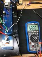
I have my F6 right channel pcb powered up with +/-25 VDC but I have zero bias across the 0.47 ohm resister at R2. I'm using a 6.1 V zener. All other components are per 6L6 's Build Guide. I thought I read somewhere that one of the 10k ohm resistors might need to be changed to a lower value. Could this be my problem? Or should I change the zeners to 5.2 or 5.6 V? Any help would be greatly appreciated.
John
John
If the voltage across the 6.1v Zener is lower than around 6.1v, R7 and R8 aren't allowing enough current to go through the Zener to reach the 6.1v. The 10k ohm resistors need to be changed with something like a 3.3k. Leave the 6.1v Zener in place. it shouldn't cause any issues.
Also, don't forget to turn the pots for the bias back down before you start it up in case you change the resistors out.
Also, don't forget to turn the pots for the bias back down before you start it up in case you change the resistors out.
VDC across Bias zener with positive lead on cathode = +5.855. VDC across Bias zener with negative lead on cathode = -5.855.pics, and measure voltage across zeners, both up and down
write here
VDC across Offset zener with positive lead on cathode = +5.909. VDC across Offsset zener with negative lead on cathode = +5.910.
RCA input wires are not connected and taped off. Speaker output wires are not connected and taped off.
Thank you for your help,
John
Attachments

Thanks Mike,If the voltage across the 6.1v Zener is lower than around 6.1v, R7 and R8 aren't allowing enough current to go through the Zener to reach the 6.1v. The 10k ohm resistors need to be changed with something like a 3.3k. Leave the 6.1v Zener in place. it shouldn't cause any issues.
Also, don't forget to turn the pots for the bias back down before you start it up in case you change the resistors out.
I suspected those 10k resisters are preventing the zeners from turning on. I don't have any 3.3k resistors, but I could parallet resistors that are approximately 5k ohms to reduce the resistance to approximately 3.3k.
John
Correction: VDC across Offset zener with negative lead on cathode = -5.910 (not +5.910).VDC across Bias zener with positive lead on cathode = +5.855. VDC across Bias zener with negative lead on cathode = -5.855.
VDC across Offset zener with positive lead on cathode = +5.909. VDC across Offsset zener with negative lead on cathode = +5.910.
RCA input wires are not connected and taped off. Speaker output wires are not connected and taped off.
Thank you for your help,
John
- Home
- Amplifiers
- Pass Labs
- F6 build