Mr. Pass suggested in a past post [Nov. 2, 2007] that F6 will be a 100 W Monoblock. He also wrote that there will be an F7 and an F8. More therapy and fun for years to come!probably Pa just changed his mind in a meantime , regarding F nomenclature and actual 6-th amp
Mr. Pass is very serious person , when biz is in question ........
luckily , mocking Greedy Boyz isn't biz for him , so we can't expect same sort of seriousness

luckily , mocking Greedy Boyz isn't biz for him , so we can't expect same sort of seriousness
Sounds about right, but more devices will be required for 100W class-A and no more than 35W/device. Need at least 2.5A bias. At least 3 pairs of devices are needed.
use 2 pairs of outputs , up PSU to +/-50V , keep static dissipation per device under 35W and
Pls goto Thread F6 post #8 by Mr. Pass. Plans may have changed.

Five years is several lifetimes in a design cycle. I have no recollection of
what that F6 was.
In any case, 100 watts is do-able, but practically speaking it's not really
worth the effort to get beyond 40 to 50 watts with this design.
😎
what that F6 was.
In any case, 100 watts is do-able, but practically speaking it's not really
worth the effort to get beyond 40 to 50 watts with this design.
😎
Practical😀
Hey Nelson, how does this compare to the J2 considering the like devices used? Gotta decide whther to give it a go.
Hey Nelson, how does this compare to the J2 considering the like devices used? Gotta decide whther to give it a go.
use 2 pairs of outputs , up PSU to +/-50V , keep static dissipation per device under 35W and
Please see the attached file for another possible option to boost power of the basic Conceptual F6 and its clones if needed. I am borrowing the established approach of the classic STASIS {R} technology invented by Mr. Pass. I am describing a powerful Class AB power amp with a potential Class A performance.
Both JFETs are operating in a highly linear state. The upper JFET and its bootstrap multiple PNPs are operating in true STASIS{R}. The JFET is a linear voltage source amp controlling a much more powerful transconductance amp [the PNPs operating in the common source configuration] which are on the verge of conduction in their idle state. In operation, this net combination is a powerful voltage source amp [and very low output Z] which does not need corrective loop feedback at all because the upper JFEt is close to being error free by design [the invention].
The lower JFET is also operating in a highly linear mode. It drives multiple NPNs [complementary to upper PNPs and also operating in the common source configuration. This arrangement is not STASIS{R} like the upper section; because the lower JFET is not complementary to the upper JFET. So the lower JFET does not correct for error introduced at the output node due the bootstrap NPNs. But,; note these two relevant connections:
- The upper STASIS{R} section still monitors and corrects for error due the lower NPN bootstrap transconductance amp at the output node. The upper JFET does not know where any error [distortion] is coming from. If the upper JFET is designed to do a great job at error correction for both the upper and lower bootstrap BJTs, then no loop feedback will be required at all to get high power and low output Z simultaneously.
- Still have the added option to practice loop feedback to do more error correction if needed.
Attachments
Last edited:
I agree. Unfortunately, no STASIS{R} with your power boost option. STASIS{R} is powerful!copy upper one to lower one
then you have something in line with F6
Last edited:
May also consider driving 2 normal [whatever this means] F6 clones with a third Jensen; adjusting for the proper phase of the secondaries to get the +/- INputs.The obvious, but not cheapest, way to get more power and lower THD is an F6-Balanced.
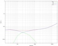
Take 2 "normal" F6 channels with balanced inputs In+ and In-, and connect the outputs Out+ and Out- to the speaker. Here is a simulation THD vs Frequency sweep:
Last edited:

- Home
- Amplifiers
- Pass Labs
- F6 Amplifier