ekobi, Don't feel too down about this. DIY can be an adventure. On the bright side the mosfets are not expensive components and can be easily replaced. See Nelson's post regarding the P channel mosfet IRFP9140: https://www.diyaudio.com/community/threads/f5m-kit.408290/post-7687559
The Vishay IRFP9140 does not have the problem that the IRFP9240 has, so the Vishay IRFP9140 is a good mosfet for the F5M.
https://www.mouser.com/ProductDetai...T*MTcxNjg0Mzk0Ny4xLjEuMTcxNjg0NDM2MS41My4wLjA.
The Q3 source to gate voltage is a bit low and the Q4 source to gate voltage is even lower. That may be due to the JFETs.
Since the other channel may now have bad mosfets, remove those mosfets, then measure the G to S voltage at both mosfet locations on the board. That will give some numbers to compare against. I would expect the voltages to be higher than 3.8V.

Matching of the P to N mosfets not required. Matching between channels also not required.
@ekobi
I sent you a PM. I have the FETs for less than Mouser and some Keratherm if you are in need. I bought Vishay 90 qty of each type 9140/140 a month or so ago.
I can totally relate to your situation and we diyers gotta back each other up. Love watching your build experience! Learning for all of us due to your sharing. Invaluable.
So many people have given me help, knowledge, parts on my journey. I'm still a noob and have a long long way to go pay it all forward and a lot more to learn from you all. Anyone need a vertical transformer mount or some wire posts? I got plenty to share for cost of shipping 😉
Generosity seems to be the foundation of keeping this entire forum thriving. Thank you to all for sharing that wherever you can!!! I gain so much value from these threads.
Edit: Apparently I have International Rectifier parts, not Vishay. I presume just as worthy though.
Generosity seems to be the foundation of keeping this entire forum thriving. Thank you to all for sharing that wherever you can!!! I gain so much value from these threads.
Edit: Apparently I have International Rectifier parts, not Vishay. I presume just as worthy though.
Last edited:
Generosity seems to be the foundation of keeping this entire forum thriving
bunch of Sissies

Just blown away by the generosity in this forum. As I mentioned to @birdbox and @ItsAllInMyHead, I was feeling pretty glum about not getting the amp up and running this weekend, but their generous offers more than make up for it. A million thanks!
I got around to dismantling the damaged audio boards this weekend. Summary of the damage
Right Channel
Most of the replacement parts arrived Friday, including a set of MOSFETs courtesy of @birdbox (thank you!). Waiting on matched set of JFETs, and then we'll give it another shot.
Right Channel
- JFETs blown
- MOSFETs apparently still operational
- R6/R7 good
- JFETs to be replaced as part of matching set
- both MOSFETs blown
- R6/R7 probably okay, but I saw them glowing red hot, so will replace
Most of the replacement parts arrived Friday, including a set of MOSFETs courtesy of @birdbox (thank you!). Waiting on matched set of JFETs, and then we'll give it another shot.
Question: any suggestions for modeling a failed JFET?
Um...it's either open or short. Not a lot of in-between.
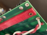
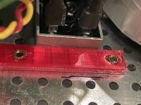
Meanwhile, I modified the PS board supports to lift the plaform a centimeter, and to optionally accommodate M3 threaded inserts. Still experimenting with fill ratios and fillets, but V4 is already much easier to work with.
Attachments

Um...it's either open or short. Not a lot of in-between.
how dare you ...... to stand against learning process?

ekobi,
Simulations in LTSpice is a great tool for helping to understand circuits.
For the F5M, I suggest you start out with R8 and R9 set to minimum value. Note Vg and Vs of mosfets and calculate their Vgs. Note the voltage drop across R6 and R7. Note the current flowing through the JFETs.
Increase the value of R8 and R8 and note the change in the mosfets' Vg. Note any changes in the voltage drop across R6 and R7. Note the current flowing through the JFETs and mosfets.
Hopefully you will see some cause and effect and get an understanding of the circuit.
An understanding of Ohm's Law is helpful, as well as understanding the relationship of Vgs of a mosfet relative to the current through a mosfet.
As far as the effect of failed JFETs, imagine if the JFETs failed open so that current no longer flows through them. What would that do the the voltage across the pots and how does that affect the mosfets' Vg and Vgs?
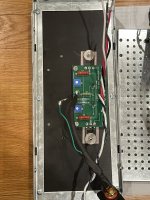
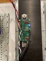
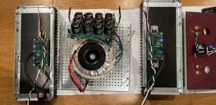
Turns out my parts had been mis-delivered over the weekend, and I retrieved them pronto. Audio boards refurbished with new FETs all around, and new R6/R7. Also simplified the wiring harnesses, switching to 14AWG for power and Vout, instead of doubled-up 18AWG -- much easier to work with.
I will now will myself to step away so I don't break it again!
I will now will myself to step away so I don't break it again!
Attachments
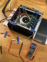
And we're making music!
I just couldn't wait to finish dialing in the bias voltages, so I plugged it into my system. Already sounds very good. Much more authoritative low end than the ACA monoblocks; excellent soundstage already, but image not as focussed as the ACAs yet, and mid-highs are "confused". But none of that stopped me from getting sucked in to listening for the better part of an hour.
I'm still trying to figure out how R8 and R9 work together to effect the biasing. I had assumed that they would modulate Q3 and Q4 more or less independently, but they clearly don't. In fact, I suspect that my earlier inability to bias the right channel was because I tried adjusting the pots in isolation. Definitely worth simulating all this to figure out how it works.
Attachments


Last edited:
They do work independently to set the mosfet gate voltages. The jfets set the current (8-ish mA) which produces a voltage across R8/R9. When both mosfet gates are driven to provide the same current through the device, voltage offset is at 0. As the N and P channel parts have do not behave exactly the same, R8/R9 require independent adjustment to arrive at a common current level.
Fried neck bones and some home fries!!!!And we're making music!
Glad it all worked out for you in the end!

My first reaction to this was going to be, "but that's not what I'm observing!", but I wanted to reaffirm my findings before responding.They do work independently to set the mosfet gate voltages. The jfets set the current (8-ish mA) which produces a voltage across R8/R9. When both mosfet gates are driven to provide the same current through the device, voltage offset is at 0. As the N and P channel parts have do not behave exactly the same, R8/R9 require independent adjustment to arrive at a common current level.
The disconnect here is that I've been monitoring the bias currents through Q3/Q4, as opposed to their bias voltages, while adjusting R8/R9. The bias currents absolutely do track each other, presumably because of the feedback loop. It's been thirty-plus years since I analyzed a circuit, and I'm obviously waaaay rusty -- time to roll up my sleeves and get simulating, I think.
- Home
- Amplifiers
- Pass Labs
- F5M build w/ Mini Disspante 3U/300