Hi
Regarding cascading the F5T.
What is the ideal voltage for the cascode transistors?
I believe the cascode voltage can be found from the voltage divider network R26 and R28:
Cascode Voltage = (Rail Voltage * R28)/(R26 + R28).
Is there an ideal voltage to aim at? From the the F5T schematic R26 = 10k and R28 = 4.75K
At 50V rails this will give a cascode voltage of about 16V and I guess leaving 50V – 16V = 34V for the fets.
At 40V rails the cascode voltage is abuot 13V leaving 27V for the fets.
Is there an ideal operating voltage for the fets?

The formula is: Railvoltage / (R26+R28) * R28. The answer is the voltage the J-fet's will see.Hi
Regarding cascading the F5T.
What is the ideal voltage for the cascode transistors?
I believe the cascode voltage can be found from the voltage divider network R26 and R28:
Cascode Voltage = (Rail Voltage * R28)/(R26 + R28).
Is there an ideal voltage to aim at? From the the F5T schematic R26 = 10k and R28 = 4.75K
At 50V rails this will give a cascode voltage of about 16V and I guess leaving 50V – 16V = 34V for the fets.
At 40V rails the cascode voltage is abuot 13V leaving 27V for the fets.
Is there an ideal operating voltage for the fets?
i would place that number a good bit below the 25V rating of the J-fet's. They do run a bit of current, so they will run hot close to maximum voltage.
So lets say 50 volt rails and R26=10K, R28=4.75K.
50 / (10+4,75) * 4,75= 16.1Vdc for the J-fets. Thats a nice figure for the J-fets to run nice and warm. But not hot 🙂
And lets say 32V rails and R26=10K, R28=10K.
32 / (10+10) *10 = 16Vdc for the J-fets.
Last edited:
Just completed assembly of my F5T v2. I set the initial bias and offset on the 1st channel and all seems to be well. I passed some music in and it seems to sound good. Now I've installed the 2nd channel. The bias on both sides (N&P) is firmly locked at 0 mV, even after several turns of the pots. The offset moved around the same way as the previous channel, i.e. a range of values up to 150 mV of so. The JFET's are hot enough that I don't want to keep my finger on them for more than a few seconds. I re-checked my stuffing and looked for shorts and I don't see anything, although I didn't remove the boards.
Any advice?
Any advice?
Burning F5t!
Hi
Once again, I will ask this great forum for advice.
Yesterday I finished my first F5T amp. After a successful F4 build I thought I would try the F5T. For both builds I have designed my own PCBs, which of course are 100% true to Pass’ schematics.
I managed to successfully adjust the bias of both channels of the F5T. I had the amp turned on for about 3 hours, to really let it cook (I’m using the U5 chassis). The bias was set at about 430mV and the DC offset was with in +-10mV. It did fluctuate some but I expect this to be normal.
Now it was time to test the amp with some music and it worked, but not without issues.
Here are the issues:
1. Hum from the speakers. I expect it to be a ground loop issue. If nothing is hooked up to the amp it is dead silent. If I hook up only 1 channel (left or right) it is still silent, but when I hook up both channels, I get hum from the speakers! The GND of the input is connected to the left and right boards respectively. The GND speaker outputs are connected to the boards (left and right respectively), and the GNDs of the boards are connected to the PSU. I have two D5-15 thermistors in series connected from GND to chassis/earth (only earth was not connected to the wall outlet). I didn’t have a CL60 available so I figured that two D5-15s (5ohm 6A) would make up a 10ohm 5A CL-60.
2. As I wanted to debug the above problem, I turned off the amp, and let it cool down for about an hour. I have a Soft Start board installed (from DiyAudio). I had no thermistor in the PSU but a 1uf filter cap (x1 or x2 I don’t remember) at the output of the Soft Start board. Besides the hum described in point 1 the 2 trafos (23Vac/16A giving me about 31Vdc rails. ) hum a little. So I decided to try to add two D5-15 thermistors in series before the Soft Start board. I also changed a cap (C2) on the Soft Start Board from 1uf to 0.33uf to increase the time before the relay sets in. Here comes the problem: As I now turned on the amp Q4 on the right channel went into flames. Literally! Hmm. I changed Q4, turned down the bias to 0 to rebias, only to have Q3 go into flames! I changed Q3 (now I’m starting to run out of matched IRFP9240s). I turned on the amp again, checked the positive rail (31Vdc) and nothing happened at first. I turned off the amp, decided to aim the bias setting at 400mV this time, thus turning down the bias on the healthy left channel so that I could also readjust the bias of this channel. With both channels having the bias set to 0 I turned on the amp and this time R13 and R14 on the left channel blew up!!!!
I’m wondering if the amp is oscillating? The value of R13 and R14 were 240ohm and I have the optional C3 and C4 1nf caps installed.
Extra info:
The boards are not cascoded.
The values of R5 and R6 (the 1k resistor parallel with the 5k pot P1/P2) were changed to 2k2 as I wasn’t able to adjust the bias to more than about 170mV with the 1k values.
If anyone can diel me in the right direction, I would be grateful.
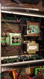
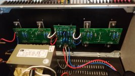
Attachments
either oscilations or initial Iq is too high
bias amp down, power on, rebias fully
measure voltages across JFet drain resistances, write down
power off , let it cool down
desolder mosfet gate leads from FE, solder them to rails (shorting G to S so mosfets closed)
power up and measure what voltage you have across JFet drain resistances, write down, post here - both hot and cold values
@foranobject, can you check what is happening at the drain of the JFET? You can probably tap that signal at the output PCBs, if you're using the store boards. It's the same signal that goes to the MOSFET gate resistors.
@sismik11, I think the recommended bias point was 350mv so the diodes wouldn't run away, which is what it sounds like happened.
Without a PCB it's almost impossible to track down your hum problem, you seem to have the external wiring correct but it looks like you have speaker return current flowing through the input wiring. You might try running a (very) thick wire between the L/R boards to force currents away from your inputs. Where to solder this wire depends on your boards.
Edit: Zen beat me to it.
What came to mind for me when reading this was what Sangram noted about the bias level.
If you read the F5 Turbo document I believe there are some guidelines on how high to go. I did not install the Turbo diodes on my V3 build. If you do the math for a V3 with 4 sets of output fets there is only a minimal gain in output power for a normal speaker load, which would typically be no lower than 3 ohms at some frequencies.
The other thing is your ps voltages are close to the recommended limit for using a cascode and perhaps with no load the voltage rises to a point where the input jfets exceeded their limits.
F5turbos are more demanding to build and adjust then other Pass DIY projects. When you get a catastrophic failure like this you need to find out exactly what happened to prevent a repeat performance by the magic smoke when you power on the next time.
I completely missed the fact that boards weren't cascoded. As far as I'm aware there's no current F5T schematic that has the diodes, but not the cascode.
I've also never built any of these with the diodes, and I've never needed to. There's more than sufficient current without. I assume if you're running 3+ pairs with 40V rails or more you'd need more current to go with the higher voltage.
Zen makes a good point about initial Iq. With thermistors in the circuit, a cold amp will have about 10-20% higher bias than a hot amp depending on sinks, so if the amp was left to cool with 450mV hot bias (which is already at the conduction point for the diodes), the diodes would be fully switched on in a cold amp.
As far as I'm aware there's no current F5T schematic that has the diodes, but not the cascode.
From the article - V2. Only the V3 has the cascode in the article.

Papa is originator of FAB Club and sole worthy member
aware or not, Greedy Boyz are Sissies, better to use cascodes
contrary, it always ends with crying in public
aware or not, Greedy Boyz are Sissies, better to use cascodes
contrary, it always ends with crying in public
Thank you all.
I have made my PCBs so that I can do with or without cascoding. I think I will try cascoding. Also it sound like taking out the diodes might make the amp easier to work with, is this correct? , and I will limit the bias to 350mV.
I have made my PCBs so that I can do with or without cascoding. I think I will try cascoding. Also it sound like taking out the diodes might make the amp easier to work with, is this correct? , and I will limit the bias to 350mV.
Folks:
I'm making good progress on my F5T V3 repairs (see post #6165). One of the benefits of having built V3s is that I have a pair of extra front-end boards; after determining that all of the active components and many of the resistors on my blown front-end board needed replacement, it was easier to simply build a replacement board.
But I also found two of the FQA19N20 had fried on the pair of N-channel output boards, and the four 47R resistors on those two boards were either mildly singed or starting to fall apart. I had an extra quad of the '19N20s and replaced those resistors as well (the other resistors on those output boards looked and tested just fine).
I just finished examining the P-channel output boards. The quad of FQA12P20 look fine, but the 47R resistors on that side of the amp look mildly singed (perhaps not as bad as the N-channel side but still worthy of replacement).
The 47R resistors on my N-channel and P-channel output boards are all 0.25W PRP resistors. I don't have any higher-wattage 47R in stock but do have enough 100R 0.5W resistors available. If the problem with R13-R16 on the output boards is that I needed higher wattage resistors all along, paralleling two 100R 0.5W would presumably work. On the other hand, if the 47R resistors were damaged at the same time as the front-end board, then I assume 0.25W resistors are adequate.
I'm terrible at diagnosing problems like this. Am I on the right path, and what do you suggest I do?
As always, thanks for the input!
Regards,
Scott
@foranobject, can you check what is happening at the drain of the JFET? .
With P1& P2 set to 0 Ohms, I measured ~66 mV at Q1 (which seemed to be slowly increasing) and ~70 mV at Q2. Both relative to ground.
That doesn't sound good, your MOSFETs would have punched through with this amount of juice. The MOSFET bias is basically (supply voltage - gate voltage), which in a build without cascodes would be the same as the JFET drain. Even with cascodes, you should have between 8 and 12 volts here.
Again, I am hoping these weren't drain readouts - source readouts would be around this level for ~6.5-7mA current through the devices. If your front end is operating normally you should have supply voltage on both sides of the pot at zero pot position, and on the drain of the JFET (or the collector of the cascode). Can you check if you get this? You should recheck the pots by measuring zero ohms across it.
Scott, you seem to have come across the same error I ran into while troubleshooting some amps built here when built with tiny JFET source R + no cascodes + diodes, destroyed N-JFETs, and cooked gate resistors and output devices. The only solution I can offer is a ground-up rebuild with cascodes with small capacitors across the feedback resistors.
At a calculated risk of contravening the schematic, I also use the 'older' F5-vanilla style thermistor layout and don't use the diodes, and at the same time retain the current limiter from the original - with the current limit set to about 7A per device. You are free to call me 'fraidy cat, but temperatures in India are extremely high and speakers are extremely expensive, so better safe than sorry.
In order to somewhat mitigate the thermistor's influence on sound quality (if any) I use a small cap to bypass it - around 1nF seems right. This also functions as a stabiliser and allows me to resize the feedback components. My oldest amp has been running hard for six years now with nary an issue, and I've built quite a few for friends. No complaints so far, though in some of them I use lateral MOSFETs (with appropriate changes) to simplify the implementation.
Last edited:
Sangram:
Thanks for the response. To be clear, my F5T V3 amps had cascodes. And what I'm in the process of doing is a semi-rebuild: the front end board on the blown amp has been replaced with an entirely new board. I've replaced the four N-channel MOSFETs and the small resistors on the output boards, but the four MUR3020 diodes and 1R 5W resistors all test fine.
Now, I'm considering removing the just-replaced 47R resistors on the output boards with higher-wattage resistors. If this is a reasonable idea, would 1W resistors be adequate?
Whatever upgrades are implemented on the blown amp will, naturally, also be performed on the working mono block.
You mentioned putting small caps across the feedback resistors. I'm game to try it. Can you suggest a value and cap type?
Thanks again for the input!
Regards,
Scott
Sorry, Scott, I must've gotten confused with the number of variations. Yes, the diodes never blow and because they strap across the resistors, those never blow either, being limited to extremely low dissipation. I prefer having blown resistors to having blown devices, FWIW. They're cheaper, easier to remove because of one less lead, and less of a hassle to procure and match.
One way to get more bias out of this circuit before allowing diode conduction is to lower the effective source resistors, from 2x1R to 3x 1R in parallel. This allows to get a little more headroom before diode conduction, potentially also allowing for a slightly higher temperature headroom (the diodes conduct better as they get hotter, we're trying to push this further out). Obviously your target bias voltage will reduce by 33% because of this change.
The gate stoppers should not need higher wattage if the front end is stable. I use 250mW Beyschlag surface mount types and they're more than adequate. In fact it is probably best to leave these resistors small, there's no upside to upsizing them. I also use a gate protector on the input JFETs just in case, it's two 9.1 zeners back to back across the input. If your stability is marginal I would also use a zener protector across the MOSFET gates. This is basically a 12V zener and a 1N4148 that clamps the MOSFET gate and protects the MOSFET gate a bit better.
The 10R resistors obviously need to be 2W types, as mentioned earlier. I use 30W Caddocks here. My feedback combination is 220pF across a 100ohm resistor, but I would recommend a minimum of 470pF as I have other stability measures in place. The article, or the original thread, has it at 1nF. Any metallised capacitor is fine, a film and foil probably the best for HF stability. C0G or NP0 ceramics will also work.
All of these measures will reduce the amplifier's bandwidth. The F5/Turbo is run with no compensation and very small stage count, to enable a wide bandwidth without resorting to tons of negative feedback. However all devices are intrinsically very high bandwidth, and you could run into potential stability issues at any time. You don't have to do everything I mentioned here - start with just the caps across the feedback resistors, and see how it goes. If you are feeding this from any kind of high voltage preamplifier, I would also move to protect the input JFETs. These two changes should have you covered for almost any kind of issue.
- Home
- Amplifiers
- Pass Labs
- F5 Turbo Builders Thread