Nelson Pass said:
By experience, I know you will get a significant effect by exploring
the Mosfet Gate stoppers. They like to be low, but you have to
balance that against the possibility of parasitics.
Absolutely. You already pointed out this behaviour in this forum.
In the F5 schematics you indicated the Mosfet gate stopper as low as 47 ohms, but in the close up published by 6moons the Nch Mosfet seems to have a 150 ohms resistors at its gate.
I'm wondering why.....
jackinnj said:There are two peaks, and it seems to relate to stray input capacitance and the value of the input resistor.
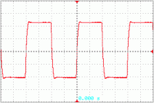
So I picked a convenient channel and looked at the square wave
at 100 KHz while playing with the Mosfet Gate stoppers and the
Jfet input resistor.
Reducing the input 1K to 820 ohms gave me a slight improvement in
overshoot and increased the slew rate slightly. Going to a lower
resistance increased the overshoot. Frankly, I don't see a
compelling reason to change the 1K value unless you are dealing
with an amp which has severe overshoot.
I varied the values of the Mosfet Gate resistors between 47 and 150
ohms. It didn't make enough difference to comment on, but I have
seen it have an effect before, so you wouldn't want to rule it out.
Of course a small capacitor to ground at the JFET gate kills the
overshoot nicely. A few pF does the trick.
Here's a 100 KHz scope photo with the 820 ohms, no capacitor,
and 75 ohm Mosfet Gate stoppers
Attachments
Re: My F5
General consensus is that thermal coupling of input JFETs should be provided for. Otherwise, nice ! 😉
masterat said:This my F5 any suggestion?
General consensus is that thermal coupling of input JFETs should be provided for. Otherwise, nice ! 😉
re: f5 PCB
Juma,
This prints out nicely, but too large.
What are the dimensions supposed to be? I will shrink to fit.
My intention is to get this schematic stuffed into a 2" x 6" PCB.
Juma,
This prints out nicely, but too large.
What are the dimensions supposed to be? I will shrink to fit.
My intention is to get this schematic stuffed into a 2" x 6" PCB.
Re: re: f5 PCB
Read my mail again 😉
It's 9.9 cm x 3.5 cm (1" = 2,54 cm)
mithomas said:Juma,
This prints out nicely, but too large.
What are the dimensions supposed to be? I will shrink to fit.
My intention is to get this schematic stuffed into a 2" x 6" PCB.
Read my mail again 😉
It's 9.9 cm x 3.5 cm (1" = 2,54 cm)
Re: F5 PCB
😀
now - that's really fugly!

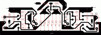
juma said:Another F5 PCB layout (the last one, I promise 😀 ). All mistakes are cured, pinouts are OK. It's a copper side view, dimensions are 9.9 x 3.5 cm.
😀
now - that's really fugly!
Re: Re: F5 PCB
Yes, maybe even bfugly 😀
Zen Mod said:
😀
now - that's really fugly!
Yes, maybe even bfugly 😀
Re: F5 PCB
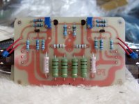
Nice Board Juma : mine is in acid right now
😎
juma said:Another F5 PCB layout (the last one, I promise 😀 ). All mistakes are cured, pinouts are OK. It's a copper side view, dimensions are 9.9 x 3.5 cm.
Nice Board Juma : mine is in acid right now
😎
Re: Re: My F5
Do complementary device need thermal coupling?
I know you would want to do so if they are both
same channel type.
juma said:
General consensus is that thermal coupling of input JFETs should be provided for. Otherwise, nice ! 😉
Do complementary device need thermal coupling?
I know you would want to do so if they are both
same channel type.
Re: Re: Re: My F5
Good ! How do they look ?
Mine are out of acid, and stuffing is on the way (see attachment - still waiting for FQA 12P20 and power resistors, but I succeeded finding two pairs of J74BL / K170BL)
Thermal drift hits silicon without knowing it's gender 😀
stefanobilliani said:
Nice Board Juma : mine is in acid right now
😎
Good ! How do they look ?
Mine are out of acid, and stuffing is on the way (see attachment - still waiting for FQA 12P20 and power resistors, but I succeeded finding two pairs of J74BL / K170BL)
coloradosound said:
Do complementary device need thermal coupling?
I know you would want to do so if they are both
same channel type.
Thermal drift hits silicon without knowing it's gender 😀
Attachments
Re: Re: Re: My F5
think about offset ;
even if I think that in Papa's handwork they aren't kissing each other .....
coloradosound said:
Do complementary device need thermal coupling?
I know you would want to do so if they are both
same channel type.
think about offset ;
even if I think that in Papa's handwork they aren't kissing each other .....
Re: Re: Re: Re: My F5
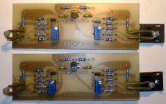
They arent out yet ; also waiting for the J74 to come , and need to find the thermistor . All the other parts are ready . Chassis and heatsinks included . Mmmmm I will install also a stereo log pot .
😎
juma said:
Good ! How do they look ?
Mine are out of acid, and stuffing is on the way (see attachment - still waiting for FQA 12P20 and power resistors, but I succeeded finding two pairs of J74BL / K170BL)
They arent out yet ; also waiting for the J74 to come , and need to find the thermistor . All the other parts are ready . Chassis and heatsinks included . Mmmmm I will install also a stereo log pot .
😎
Re: Re: Re: Re: Re: My F5
Why is it taking so long ? I etched mine PCBs in 2-3 minutes with 10% HCl solution and 8% H2O2.
stefanobilliani said:
They arent out yet ; also waiting for the J74 to come , and need to find the thermistor . All the other parts are ready . Chassis and heatsinks included . Mmmmm I will install also a stereo log pot .
😎
Why is it taking so long ? I etched mine PCBs in 2-3 minutes with 10% HCl solution and 8% H2O2.
I dont know , but its taking too long infact and I am a little worried for the traces . I went to the electronic store for a prepared acid . It is 60% Ferric chlorid crystal ( FeCI3 6H2O ).
Re: F5 PCB
juma, (the last one, I promise 😀 )
If possible could you send me the layout file, again?
juma said:Another F5 PCB layout (the last one, I promise 😀 ). All mistakes are cured, pinouts are OK. It's a copper side view, dimensions are 9.9 x 3.5 cm.
juma, (the last one, I promise 😀 )
If possible could you send me the layout file, again?
Re: Re: F5 PCB
Here it is - zipped layout file from Sprint-Layout 5.0
mike_diy said:
juma, (the last one, I promise 😀 )
If possible could you send me the layout file, again?
Here it is - zipped layout file from Sprint-Layout 5.0
Attachments
stefanobilliani said:I dont know , but its taking too long infact and I am a little worried for the traces . I went to the electronic store for a prepared acid . It is 60% Ferric chlorid crystal ( FeCI3 6H2O ).
The brown stuff ? 25 years ago, barely teenager, I had bad experiences with it (etching lasts forever, stains on clothes won't come out...) and I never used it again - it's pain in the neck !
juma said:
The brown stuff ? 25 years ago, barely teenager, I had bad experiences with it (etching lasts forever, stains on clothes won't come out...) and I never used it again - it's pain in the neck !
yes youre right , I will not use it anymore .
😡
edit : reading that and the etching thread it seems I am a bit late with this , but I'll change , promised , no more brown stuff .

- Home
- Amplifiers
- Pass Labs
- F5 power amplifier