Congrats!
(again)
and thank you for sharing your passions and assistance to us all.
Best,
Chris
(again)
and thank you for sharing your passions and assistance to us all.
Best,
Chris
That is a great review, a deserved flower for First Watt and Mr. Pass.
I'm working on this one Nelson... and thanks again for sharing so much.
😎
I'm working on this one Nelson... and thanks again for sharing so much.
😎
Very nice review, so I definitely need to get hopping on mine.
New stuff also up a couple days ago on the FirstWatt site, but the link to the F5 manual doesn't seem to work today.
http://www.firstwatt.com/downloads/F5-om_sm-080527.pdf
The other to the AX article/tutorial works fine.
Thanks again for sharing this. Can't wait for the "B" products too. It should keep the faithful entertained and stimulated for some time.
Tom
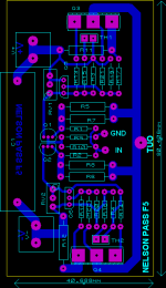
Hi Goffe,
If you want Q1 and Q2 placed face-to face, than the D and S of Q2 should trade places.
The IN and GND points too.
R1 and R2 should be at least 1W.
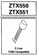
ZTX 450/550 have Collector as the middle pin.
What's C1 ?
Keep working, your PCB is getting better and better !
🙂
If you want Q1 and Q2 placed face-to face, than the D and S of Q2 should trade places.
The IN and GND points too.
R1 and R2 should be at least 1W.
ZTX 450/550 have Collector as the middle pin.
What's C1 ?
Keep working, your PCB is getting better and better !
🙂
ZTX 450/550 have Collector as the middle pin.
I think ZTX 450 and 550 has BASE at the middle pin ;
With the printed face in front of you ,the left pin is collector .
juma said:Hi Goffe,
If you want Q1 and Q2 placed face-to face, than the D and S of Q2 should trade places.
The IN and GND points too.
R1 and R2 should be at least 1W.
ZTX 450/550 have Collector as the middle pin.
What's C1 ?
Keep working, your PCB is getting better and better !
🙂
Q2,IN, GND you are right juma, thanks!
My mistake

C1 are bipass cap from V+ to V-(maybe not necessary)
juma said:
R1 and R2 should be at least 1W.
??? 😕 ???
Why?
8 mA in each resistor squared * 10 ohms
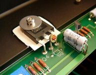
Did anybody noticed that in the close up picture in post #926 at the top of this page Nelson added a 2.4 ohms resistor in parallel to the 0.47 ohm source resistor of the Nch mosfet (Q4)?
Moreover, the gate resistor seems to be 150 ohms in lieu of 47 ohms indicated in the published schematics. (Assuming that the left hand resistor close to the gate is R14)
A special tweaking or........???
Moreover, the gate resistor seems to be 150 ohms in lieu of 47 ohms indicated in the published schematics. (Assuming that the left hand resistor close to the gate is R14)
A special tweaking or........???

I'm sure the Master tweaks all of the production units.
R1 andR2 are also part of the 60 ohm feedback loop, try that with 20V across it.
Bill
R1 andR2 are also part of the 60 ohm feedback loop, try that with 20V across it.
Bill
stefanobilliani said:
I think ZTX 450 and 550 has BASE at the middle pin ;
With the printed face in front of you ,the left pin is collector .
Yes, the base is in the middle, but with the printed face in front of you , the right pin is collector (picture from datasheet attached)
massimo said:
??? 😕 ???
Why?
8 mA in each resistor squared * 10 ohms
You forget the current that is coming from output through 100 Ohms / 3 W resistors.
Attachments
philosopy about input sensitivity vs output?
Could someone please elaborate about the current prevailing philosophy
of input sensitivity vs output wattage and specs, with any technical
justification for this position? I'm just a hobbiest. I'm not a EE. I'm
not trying to agrue any position. I am hoping to gain an understanding
of the issues.
Again, I'm not a EE, so please feel free to correct any of my mistakes.
Here is my understanding of the situation:
By my simulation, with a 1.5V input (3Vpp), and an 8 ohm load, this amp
outputs about 12V (22Vpp). 12V * 2.6A = 31.2W, what I think would be
considered peak. 31.2W * .707 = 22W RMS. So with an input of 1.5V,
we get an output of about 22W RMS. I'm not sure if discussing the
simulator's predicted distortion measurements is valuable, so let me just
say that the simulated circuit's THD measurement is in the same
ballpark as what Nelson published.
Now 12V is obviously no where near the 24V rail voltage, and the amp
is not clipping at the 1.5V input. The amp is getting close to clipping
at an input around 3.7V (7.4Vpp). At 3.7V input, we get about a 22V
(44Vpp) output, with distortion in the ballpark of .5% (again, simulated).
22V * 2.6A = 57.2W peak. 57.2W * .707 = 40W RMS.
I'm under the impression that most amps have a specified full output
rating with an input of around 1.5V. Or at least many give their specs
that way. I'm not saying that one should judge amps on their specs alone,
but I use specs to get me in the ballpark of devices I want to compare.
One viewpoint is that this amp is a lot more powerful than a 22W amp.
Should we say that this is a 22W amp with almost 3dB of headroom?
Another observation that is really interesting to me is that the 3.7V input
that led to the output being slightly shy of clipping in the F5 is exactly the
same as what was designed for the Zen 5. This makes me think that
Nelson has a philosophy about input and output ratings.
So it seems to me that there are many different ways, and each way
could be factually correct, that one could give specs or generally
classify an amp. It also seems to me that Nelson has a design
philosophy that he uses in this regard. Would anyone care to explain
this philosophy, including a technical justification for this position? It
probably wouldn't take too deep of a technical discussion to loose me.
But if I don't ask, I may never know...
thanks,
Robert
juma said:
You forget the current that is coming from output through 100 Ohms / 3 W resistors.
Yes, you're right.
It doesn't look Nelson has used other than Dale RN55 resistors at the input of the amp reviewed by 6moons, anyway. (the two + two resistors close to the JFets, iI mean.)
Even in the article, a part from the blue Pana 3W, he suggested to use 1/2 W resistors throughout.
Nelson Pass said:
The closest I've got is to get a 1 dB peak at about 800 KHz.
There are two peaks, and it seems to relate to stray input capacitance and the value of the input resistor.
Stray input capacitance -- my bad -- I should have remembered that it quacks like a current feedback opamp so it's some sloppiness in the layout, even a few pf's causing peaking. Viewers are strongly advised of the adult nature of the material which will appear on your screen:
An externally hosted image should be here but it was not working when we last tested it.
That's out to 2 MHz.
That's really interesting. Frankly, I didn't put any thought into
the input resistance vs bandwidth - I simply defaulted to the
known "won't oscillate" values at the Gates of the JFETs.
My actual circuits don't correspond to these results though, so
I'll take the time to play with it and come back with some info.
the input resistance vs bandwidth - I simply defaulted to the
known "won't oscillate" values at the Gates of the JFETs.
My actual circuits don't correspond to these results though, so
I'll take the time to play with it and come back with some info.
The bandwidth will also be a function of the feedback resistance.
It's not that my layout is sloppy per se, it's just that not enough consideration was given to the capacitance issues. I will try doing this "dead-bug style" with some 50 ohm coax rather than Pomona clips, maybe another using surface mount input resistors to each of the gates.
It's not that my layout is sloppy per se, it's just that not enough consideration was given to the capacitance issues. I will try doing this "dead-bug style" with some 50 ohm coax rather than Pomona clips, maybe another using surface mount input resistors to each of the gates.
- Home
- Amplifiers
- Pass Labs
- F5 power amplifier