
Back on topic
1 I am not going to even think about posting how a turbo works....
As long as it does not spoil the engine sound in this case.
2 I most certanly not going to even try to think about triing to think about what PAPA GOT IN STORE
I am one of the Happy Ignorant ones that get blown off by litle things such as P3.
Tanks Papa it Is.
Last edited:
If you bend the legs in the flat (easy) direction , one forward and one back so they look like they're running, they'll work I'm pretty sure as a friend of mine did exactly that..and it looks just fine when they're done. The resistors don't need very big sinks, just squares of aluminum do it..
Mark
Mark
Hi,
I bought parts and Caddock resistors from tech-diy for my diyaudio P-F5-2V20e based F5.
I intend to use a small heat sink for the R1, R2 resistors but am unsure what I should do with the others. The layout of the board does not allow placing them on the main heatsink, unless the leads to R5, R8, R11 and R12 are extended using wires. Can extending cause problems?
Thanks,
Albert
The resistors don't need very big sinks, just squares of aluminum do it..
Mark
As in Mouser part number 532-6043PB or Digikey HS216-ND. The latter may not fit some of the larger Caddocks but does work fine on the 15W Caddocks such as the MP915s of the MP900 series. E.g., the MP915-50.0-1% which works well as a 50R feedback resistor to replace R5||R7 and R6||R8. I myself wouldn't bother with heat sinks for R1 and R2, but using them certainly can't hurt either.
Dan
Biasing problem
I have just started trying to bias my F5 mono blocks... only problem is I'm not seeing any voltage on my R111 R112 resistors. I have my pots turned to zero by checking across R3 and R4. When I turn them up the DC on the output changes but I see no voltage across R111 or R112. Same thing happens on both amps. I'm getting 25.5 volts at the board and the LED I have installed lights.
Any ideas what I should start checking first? These are Christians v2 boards from about a year ago.
erpiii
Attachments
check the limiting transistors. Maybe they are conducting (shorting). Some have inserted these the wrong way around/different type used.
check the limiting transistors. Maybe they are conducting (shorting). Some have inserted these the wrong way around/different type used.
Unless the boards are marked incorrectly, they (ZXT450/550) appear to be installed correctly. I also checked Q1 and 2 and they also look correct.
I used other boards. Others have hands on on these PCBs you have.
What is the max voltage over the drain resistor (thus P1/2)? If it is max 0,6 V check the pinout of the ztx's again . .. At 0,6V the IRF's just conduct a trickle.
- the DC changes so there is a loop - even if it is mA's.
What is the max voltage over the drain resistor (thus P1/2)? If it is max 0,6 V check the pinout of the ztx's again . .. At 0,6V the IRF's just conduct a trickle.
- the DC changes so there is a loop - even if it is mA's.
Do you have something connected at Q101 & Q102 as there appears to be solder on the pads at there position?
Do you have something connected at Q101 & Q102 as there appears to be solder on the pads at there position?
If the Id starts to flow, but never reaches the threshold for the IRF to [really] conduct, then the Idss of the inputs (2sk170/2sj74) is too low --> raise the drain resistor, so the max voltage drop will increase.
I circumvented this type of problem by first determining the Vgs of the outputs and then (2) seeing - on the half-built board, no outputs yet - what the Vd referenced from the V+ or V- is. [Then you can swap resistor R3/4] You should be able to get the required Vgs at ease, then return P1/P2 to zero and connect the outputs.
2 ¢ please 😉
Tweaked it to include resistors in the arms of P3 to prevent one side or the other from bottoming out as AndrewT had suggested.
The boards have pads for SMT JFETs including the BF862, PN4393, J176. Note that the BF862 has a different SOT pinout than the others. The Caddocks, optionally, can hang off the bottom of the board and be attached directly to the heat sink without the need of any gymnastics in wiring.
Boards measure 4.500x2.000
The boards have pads for SMT JFETs including the BF862, PN4393, J176. Note that the BF862 has a different SOT pinout than the others. The Caddocks, optionally, can hang off the bottom of the board and be attached directly to the heat sink without the need of any gymnastics in wiring.
An externally hosted image should be here but it was not working when we last tested it.
An externally hosted image should be here but it was not working when we last tested it.
Boards measure 4.500x2.000
Jack,
If you move the R1 & R2, then all the 4 to-220 input jfets can be moved together and physically connect them on a common small copper strip for better heat tracking -
I made up an insulated thin copper strip and bolted it to the heatsink so it reaches across the width of the pcb and the jfets operate at nearly the heatsink temp - it sounds better, IMO.
just the 2c!
To220 input devices?
Those shown are To92 inputs.
Yes, they could be thermally coupled with a strip of aluminium or copper clamped between the flat faces
The SMD (SOT 23, etc.) could be located such that a copper trace acts as a PCB heatsink to help thermally couple them. Note that the upper pair and the lower pair have common drains and common sources. If these traces are kept very short they will offer some thermal coupling.
I used other boards. Others have hands on on these PCBs you have.
What is the max voltage over the drain resistor (thus P1/2)? If it is max 0,6 V check the pinout of the ztx's again . .. At 0,6V the IRF's just conduct a trickle.
- the DC changes so there is a loop - even if it is mA's.
Laff... I just look at the pictures and place the components... I have no practical knowledge about electronic circuits or what could be wrong. I guess I'll just buy another kit and try to replicate the process again and see if it works right the next time. Even a blind squirrel can find a nut if he looks long enough.
erpiii
The ztx aren't compulsary. (limiters)
You could take them out and see if it works.
If it does work then it will mean they were wrongly wired.
You could take them out and see if it works.
If it does work then it will mean they were wrongly wired.
Tweaked it to include resistors in the arms of P3 to prevent one side or the other from bottoming out as AndrewT had suggested.
...
Boards measure 4.500x2.000
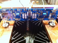
As long as you're going for small boards, you might consider if you want to put the output devices on opposite ends of the board. This then accommodates clamping the boards to heatsinks with parallel T-slots. Aavid Thermalloy, Fischer, and Wakefield makesuch heatsinks with 80mm spacing (on center) between the T-slots. These work well with Michael Rothacher's Circolotron design as well as Peter Daniel's F5 PCB. The following image is of a Peter Daniel F5 PCB clamped to a 0.31C/W Aavid Thermalloy heatsink whose face measures 125 by 180mm. (Newark*10WX1020 or 10WX1015; Farnell 170753 or 179956.) As an aside, a fairly compact stereo F5 enclosure can be made using these heatsinks if you put most of the PSU in a separate enclosure (xformer, rectification, and first two stages of a CRC filter).
An externally hosted image should be here but it was not working when we last tested it.
Dan
I created a composite SMT/Through Hole Device for the JFETs and snugged them up:
An externally hosted image should be here but it was not working when we last tested it.
Do you have something connected at Q101 & Q102 as there appears to be solder on the pads at there position?
I had originally installed them wrong when I installed them the first time. I pulled them and reinstalled them in the correct Q1/Q2 spots before i powered up the boards... I guess I could have over heated them by doing that. Should pull them and test them. Can anyone tell how to test the 170/j74 fets?
erpiii
check the limiting transistors. Maybe they are conducting (shorting). Some have inserted these the wrong way around/different type used.
Seems like I remember an issue early on with the cviller boards and reverse orintation of the zetek devices? Its been a while, but it may bear checking it out.
Russellc
- Home
- Amplifiers
- Pass Labs
- F5 power amplifier