r22 750
r5,r24, r25 1k
p2 500
I changed r22 for a 600 ohms resistor and the problem still there...
Playing with p2 doesn't move the voltage at the output. Is it right to have 12,16v dc at the speakers terminals?
What about the reversed voltage at the speakers terminals?
I can set the bias at 200mv across the .47 resistors with no problem.
Thanks again!
check r8/r9/p1 values, thats where i went wrong.
i used 10 ohm for r9 instead of 10k... dc offset went ballistic (as did the bias)
i used 10 ohm for r9 instead of 10k... dc offset went ballistic (as did the bias)
Thanks for the quick answer!
all the values seems to be alright....
r8 27.4k, r9 10k, p1 5k
dc volts at the output is reversed. This is wrong, isn't it?
all the values seems to be alright....
r8 27.4k, r9 10k, p1 5k
dc volts at the output is reversed. This is wrong, isn't it?
there should be more or less no dc at the output, only a couple of millivolts (well, thats what i get). unfortunately im not to much of a technician so i can only tell you my own experience and about the mistakes i made myself.
Your sure your fets are oke? zeners connected in the right way?
maybe you can post a picture of your f4s so we can have a look at it. there are some people with a keen eye here on the forum!
cheers,
c.
Your sure your fets are oke? zeners connected in the right way?
maybe you can post a picture of your f4s so we can have a look at it. there are some people with a keen eye here on the forum!
cheers,
c.
I am using 2SK170BL N-channel and 2SJ74BL P-channel for the input transistors, any indication in case of using these transistors? And 1N5235 (6.8v zenner) instead of 2n4736 (6.8v zenner), but this diodes are there just for protection and they should not affect to the dc offset at the output (I guess).
Vref at the TL431 is 2,49v so it is right.
I think it can't be a bad solder joint because I have the same problem on both channels, I don't know.
Maybe my IRFP's are dead.... how can I check this?
I will try to post a pic of my set as soon as I charge my camera battery...
Another clue... voltage across gates on my IRFP's are around 6v on the 9240's and 4,5v on the 240's, volts between gate and drain.
Thanks again
i agree with the soldering, having same problem on both channels would a big coincidence if it is soldering/faulty part related.
but the only way you can create any dc huge offset is via r5/r7 and r22/p2/r6 (if the fets are working properly). the rest of the circuit is decoupled via c1..c4. if you can adjust the bias and measure 200mv across all the .47 ohm resistors it seems to me fets are oke although i wouldn't know what you would measure if they were broken, that leaves the zeners... and if im wrong i hope someone will correct me!!
cheers,
c.
btw, witch version are you using, r0 6/4/07 ?
Noticed that Peter's PCB has the input go through R1 before shunting to ground via R2. Whereas the latest 6/4/07 Schematic has the Input connected to both R1 and R2 and R2 shunts to ground.
I guess by nature these 2 setups are both voltage dividers.
What's the difference between the 2 circuits?
Quoting Papa from post #397
"This version bootstraps the front end so that the JFETs only
see about 1/2 the voltage swing. It improves THD very slightly,
gets a tad more output swing, and it also extends the bandwidth
a bit. With a proper setup, I get about -3dB at 1 MHz, with a
very good looking 100 KHz square wave."
Is this what this is?
So should I cut the traces between R1&R2 & R2&D4, jumper between R1/In &R2 to achieve the latest schematic? Worth the effort?
Oops noticed that if I do that, I also need to jumper between D4 and D3/R1.
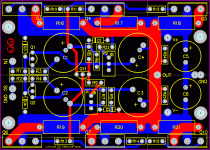
(Mods - is it ok to post the pcb attachment? Please delete if I need to obtain permission from Peter first. Thanks)
her shann
I guess by nature these 2 setups are both voltage dividers.
What's the difference between the 2 circuits?
Quoting Papa from post #397
"This version bootstraps the front end so that the JFETs only
see about 1/2 the voltage swing. It improves THD very slightly,
gets a tad more output swing, and it also extends the bandwidth
a bit. With a proper setup, I get about -3dB at 1 MHz, with a
very good looking 100 KHz square wave."
Is this what this is?
So should I cut the traces between R1&R2 & R2&D4, jumper between R1/In &R2 to achieve the latest schematic? Worth the effort?
Oops noticed that if I do that, I also need to jumper between D4 and D3/R1.
(Mods - is it ok to post the pcb attachment? Please delete if I need to obtain permission from Peter first. Thanks)
her shann
Attachments
DC offset. -12,16v
Thanks culture!
I am using r0 6/4/07, and Peter Daniel's pcb's.
I checked everything yesterday 1h30 at night...... the values where OK.... but it was too late and I was tired. I will go through it later this afternoon.
I will post pics of the setting.
Thanks culture!
I am using r0 6/4/07, and Peter Daniel's pcb's.
I checked everything yesterday 1h30 at night...... the values where OK.... but it was too late and I was tired. I will go through it later this afternoon.
I will post pics of the setting.
It seems that there is a problem with P2.
As the adjustment of P2 does not change -12.16V, the P2 must have a problem.
If P2 has the problem at the value of 500, the DC offset must be - value
because the resistance of (P2+R22) is greater than R5.
Hope you will find the problem soon.

As the adjustment of P2 does not change -12.16V, the P2 must have a problem.
If P2 has the problem at the value of 500, the DC offset must be - value
because the resistance of (P2+R22) is greater than R5.
Hope you will find the problem soon.
P2 works allright, I can pull the resistance up and down.
By the way, I am checking the dc offset on the speaker output with no load and with the input shorted. This is the right way, isn't it?
-12,16v dc output offset, could it be because a mismatch of the IRFP's?
I get different readings of milivolts across de power resistors on N's and P's, around 0,005volts diferences. Does this mean that they are not matched properly?
How can I check if any of the IRFP's are broken?
Thanks again!
hmm that sounds more than fine to me, the differences are more on my f4s 🙂
but: http://www.passdiy.com/pdf/mos.pdf
cheers
c.
but: http://www.passdiy.com/pdf/mos.pdf
cheers
c.
mongosound said:P2 works allright, I can pull the resistance up and down.
By the way, I am checking the dc offset on the speaker output with no load and with the input shorted. This is the right way, isn't it?
I think all of your mosfets are ok.
By mistake, I made one of my mosfets damaged during construction and testing, but the trouble was quite different from yours.
If the offset voltage keeps frozen despite the P2 adjustment, I would hardly believe that the P2 is working ok. It is illogic. It doesn’t matter how big the offset is. The offset voltage should be changed according to the changing P2 values. I hope you will check up once again whether all pins of the P2 are connected to the right positions.
You don't need the input shorted. Leave the input open.
Skorpio said:
If the midpoint between C3 and C4 are connected to output instead of ground the input resistance is bootstrapped and the input buffer can be left out. Also the value of c1 and c2 can be reduced....I have done that with a simular circuit with bipolars...have run superbly for years now...
Did anybody tried with the bootstrapping?
It is very easy to do.....
mongosound said:-12,16v dc output offset
I did not start to solder my f4's yet, so I do not have practice, ...
Mongosound, if you have the same phenomena at both amplifiers, maybe you made the same mistake around C1/C2 and C3/C4 and maybe D1/D2 and D3/D4:
check polarity of C1/C2 and C3/C4 with schematic and on PCB:
"+" of C1 and C3 should be on internal "+" sub-rails
"-" of C2 and C4 should be on internal "-" sub-rails
If this is okay - please remove C1 and C2 and check dc output.
Remove C3 and C4.
For sure check also "directions" (positions) of D1, D2, D3, D4. Maybe one is upside down at both amplifiers.
regards
a.
Andrzej Sochon said:
"+" of C1 and C3 should be on internal "+" sub-rails
"-" of C2 and C4 should be on internal "-" sub-rails
sorry, mistake, schould be:
"+" of C1 and C4 should be on internal "+" sub-rails
"-" of C2 and C3 should be on internal "-" sub-rails
a.
Thanks everybody, I will follow your sugestions.
I will be on vacations for the next week, so until the seventh of january you won't get news from me.
Happy new year to all of you!
Thanks again
I will be on vacations for the next week, so until the seventh of january you won't get news from me.
Happy new year to all of you!
Thanks again
happy holidays!!!
and when you're back we want some good news and pics of the amp, working or not 🙂
cheers
c.
and when you're back we want some good news and pics of the amp, working or not 🙂
cheers
c.
Am ordering the parts from digikey when I found out the all the resistor values for the particular series I'm using are available except for R8 27.4k ohm on the channel schematic.
Looking via old posts I found out that the first schematic had a R8 value of 22k and people were having problem biasing current via P1, that were cured by replacing R9 10k with 6.8k. Subsequent schematics have the R8 value at 27.4k.
So can I use a lower value of 26.7k on R8 and use P1 to dial in the bias current - P1 with a range of 5k should be able to give me a good range to play with to achieve the bias current?
thanks
her shann
hershann said:Am ordering the parts from digikey when I found out the all the resistor values for the particular series I'm using are available except for R8 27.4k ohm on the channel schematic.
Looking via old posts I found out that the first schematic had a R8 value of 22k and people were having problem biasing current via P1, that were cured by replacing R9 10k with 6.8k. Subsequent schematics have the R8 value at 27.4k.
So can I use a lower value of 26.7k on R8 and use P1 to dial in the bias current - P1 with a range of 5k should be able to give me a good range to play with to achieve the bias current?
thanks
her shann
just go for it
- Home
- Amplifiers
- Pass Labs
- F4 power amplifier