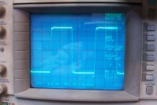
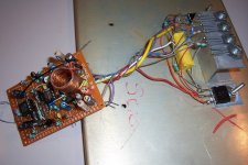
Here are a pic or two of the (now working) prototype:
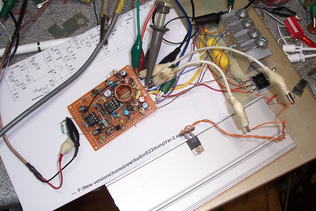
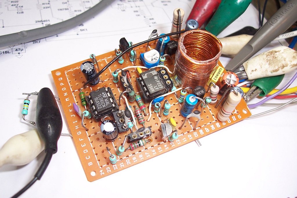
The main mods I had to carry out is to use a LF356 instead of a TL071, for HF CMRR reasons, and move the collectors of the buffer transistors at a place where they couldn't introduce a RHP zero causing instabilities.
Some verification work is still required before I can release a working, tested and provisionally definitive version.
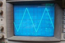
In the mean time, here are some 10kHz oscillograms showing the linearity and squarewave response (op transistors are BD249C/BD250C):


The main mods I had to carry out is to use a LF356 instead of a TL071, for HF CMRR reasons, and move the collectors of the buffer transistors at a place where they couldn't introduce a RHP zero causing instabilities.
Some verification work is still required before I can release a working, tested and provisionally definitive version.
In the mean time, here are some 10kHz oscillograms showing the linearity and squarewave response (op transistors are BD249C/BD250C):
Attachments


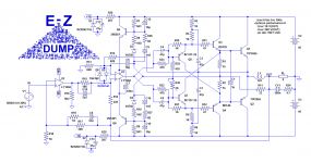
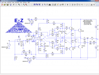
Here is the stable, tested version. It might not be optimal, but it already works well enough:

There are relatively little changes, but they have their importance: the collectors of Q7 and Q8 are now returned to the emitters of the drivers.
These are stable, low-impedance nodes which is important because the collectors carry an antiphase signal wrt. the main output, and if they are connected to the output of the class A amplifier or the class B (or C) one, they can temporarily reverse the phase of the feedback, wreaking havoc in the loop.
Other changes mainly reflect the reality of the circuit: the second stage is floating, and is at a potential close to the output, meaning all of the outside world is "hot", and injects small capacitive currents into every node.
The - input of U1 sees a relatively low impedance, and is not too affected, but the + input is more sensitive and requires a compensating cap C14 which introduces some negative FB.
Ideally, everything around U1 should be guarded by a low impedance screen connected to the potential of the inputs, but such a node doesn't exist in the circuit as it is, meaning other measures are required.
Ideally, U1 should have a good HF CMRR, something the TL071 does not have (it is not specified).
Initially, I was able to get the circuit working by substituting a LF356, but with the additional fixes, any BiFET amp now works, including the TL071.
I also tested a LF411.
The additional mods are the connection of the bootstrap caps to the class B amplifier, base stoppers for the drivers and small capacitors C15 and C16 filtering the HF out of the floating supply controllers.
All of this will be somewhat layout-dependent, because of the floating VAS, but it is a good starting point.
A reasonably compact construction would be desirable: my initial build had random flying wires connecting to the heatsink assembly, but the loop areas were atrocious and caused parasitic inductances and inductive crosstalk, resulting in low-level HF oscillations (~6MHz).
A single twist of the PCB wrt. the heatsink was sufficient to cure it.
Regarding the performance, the CD scheme seems to work perfectly: I can turn the base-spreading pot all the way without seeing any difference, and I am not going to be able to measure the THD directly.
The step response leaves to be desired, but the HF balance of the bridge can probably get a perfect response: partially inserting a ferrous tool into the 3.3µH improves the response to near-perfection: a mix of added inductance and losses.
I have included an optional pair of diodes between the inputs of U1.
They are not required for normal operation, but I noticed that bench mishaps, like a supply wire disconnecting or a probe slip could drive the circuit into latchup.
The diodes prevent such an event, and do not seem to have adverse effects.
Here is the circuit, updated with the stoppers, twist, etc.:
Attachments
Elvee, good news!
Which op amp should be LF356?
U1 only, or both HAVE TO be identical?
Correction: I can see from your photos that U2 can be different.
I'm asking because I have both:
TL071 and LF356
I also could try OPA2134, LT1056
Which op amp should be LF356?
U1 only, or both HAVE TO be identical?
Correction: I can see from your photos that U2 can be different.
I'm asking because I have both:
TL071 and LF356
I also could try OPA2134, LT1056
Last edited:
U1 is the most critical, but now with the mods any type can go anywhere.
The LT1056 is promising: it is more modern, and has better performance than the others (but I don't have one in my stock to test it).
You can install IC sockets and test a variety of different types
The LT1056 is promising: it is more modern, and has better performance than the others (but I don't have one in my stock to test it).
You can install IC sockets and test a variety of different types
There are relatively little changes, but they have their importance: the collectors of Q7 and Q8 are now returned to the emitters of the drivers.
These are stable, low-impedance nodes which is important because the collectors carry an antiphase signal wrt. the main output, and if they are connected to the output of the class A amplifier or the class B (or C) one, they can temporarily reverse the phase of the feedback, wreaking havoc in the loop.
Ahh! Makes perfect sense now.
My only remaining issue is that the pass-transistor op-amp supply does not push beyond the rails so the output inherits the op-amp voltage saturation limits plus a bit more. I would just use resistors and larger bootstrap caps, and a series resistor so that the op-amp supplies peak about 5V beyond the rails. As always, values have to be carefully chosen to avoid latch-up when overdriven.
This solution is obviously simpler, more effective and does not appear to have issues, so it looks like the way to go.
Some years ago, I opted for the active, "concertina" rails solution, and I do not exactly remember why I chose it over the ordinary bootstrap.
It could be that initially, the opamp was supposed to drive the drivers directly, without the buffer layer.
Anyway, with the current version, the plain bootstrap looks preferable.
I have tried to rationalize the circuit by using a common bootstrap for the drivers and the VAS, but it is surprisingly difficult: preventing possible latchups is absolutely nightmarish.
It could be done with additional complications, but then the dual bootstrap is more advantageous.
With the passive bootstrap, all the peculiarities of the final, working version need to be implemented, including the resistors values and ratios (necessary for the CD balance) and the FB loop encompassing the input stage (with a local loop input stage, the bandwidth is very limited, to 15 or 36kHz, I don't remember exactly).
I have rolled several opamp types for U2 (input): it tolerates significantly faster devices than the TL071, and this vastly improves the step response.
I tried a NE5534 (uncompensated), a HA-2525 (also uncompensated), and a LF357.
The FB speedup cap needs to be tweaked for optimal response: depending on the opamp, it has to be changed to 22, 24 or 27pF
Cool! Had a thought that diodes on the bootstraps could take some heat off the resistors and allow smaller bootstrap caps. Eagar to see where this goes. Note that < 50/50 bootstrap networks that only pull ~5V over can prevent rail sticking.
Cheers,
Steve
Cheers,
Steve
Last edited:
In the end, the simple passive bootstrap seems to have unexpected issues: the latchup occurs as soon as the input stage is included in the global loop, not especially with the rationalized single bootstrap I tried earlier.
I have tried to adapt the resistors R12-> R15 to keep the inputs within the supply limits, but to no avail.
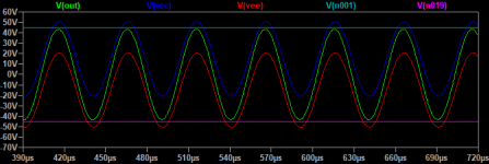
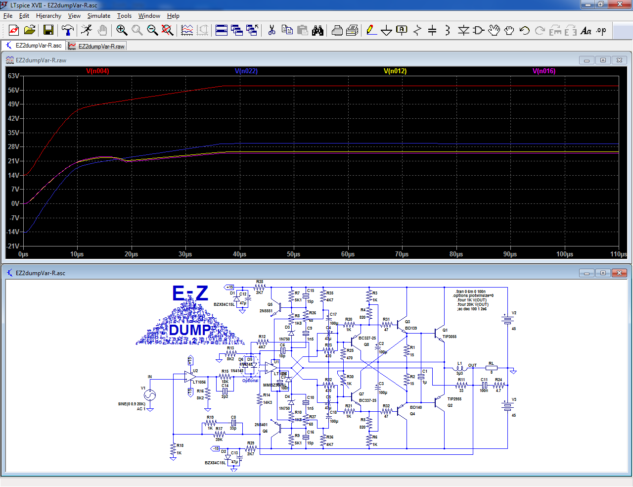
Red and blue traces are the floating supplies, yellow and magenta the inputs.
At some point, the inputs go astray and the circuit locks into latchup:
I tried the same in reality, but it didn't work better: the behavior was completely different, but completely anarchical: huge, uncontrollable oscillations, but no latchup.
By contrast, the active bootstrap remains well-behaved, both in sim and reality.
I have explored it more thoroughly and noticed that some very low-level, HF (>6MHz) oscillations could be seen at some levels, and for some wiring configurations.
They were caused by the class A amplifier, and weren't even visible in the final output, because of the inductor.
They seem to be local, limited to the driver/class A, probably because the wiring inductance doesn't mix well with the relatively high Ft of the BD139/140.
The best solution is certainly to make a proper build, on a real PCB, but some measures can cure it completely, even with my sloppy construction: mainly two 82pF capacitors to bypass the bases (upstream of the base-stoppers), and secondarily two 47 ohm in series with the bootstrapped supplies, to prevent the emitter followers from fighting with each other.
The capacitors need to be installed directly on the drivers: on the board, they become almost ineffective because of the wiring to the bases.
This is the final, most stable version:

It looks rather robust and well-behaved, and gracefully tolerates clipping and various supply voltages, but there are still some unexplained aspects, meaning the project is not for everyone: only adventurous-minded people should try it, because it could be temperamental.
It shows great promises and works exactly according to the predictions when it is stable, but it takes little to make it unstable.
I have tried to adapt the resistors R12-> R15 to keep the inputs within the supply limits, but to no avail.
Red and blue traces are the floating supplies, yellow and magenta the inputs.
At some point, the inputs go astray and the circuit locks into latchup:
I tried the same in reality, but it didn't work better: the behavior was completely different, but completely anarchical: huge, uncontrollable oscillations, but no latchup.
By contrast, the active bootstrap remains well-behaved, both in sim and reality.
I have explored it more thoroughly and noticed that some very low-level, HF (>6MHz) oscillations could be seen at some levels, and for some wiring configurations.
They were caused by the class A amplifier, and weren't even visible in the final output, because of the inductor.
They seem to be local, limited to the driver/class A, probably because the wiring inductance doesn't mix well with the relatively high Ft of the BD139/140.
The best solution is certainly to make a proper build, on a real PCB, but some measures can cure it completely, even with my sloppy construction: mainly two 82pF capacitors to bypass the bases (upstream of the base-stoppers), and secondarily two 47 ohm in series with the bootstrapped supplies, to prevent the emitter followers from fighting with each other.
The capacitors need to be installed directly on the drivers: on the board, they become almost ineffective because of the wiring to the bases.
This is the final, most stable version:
It looks rather robust and well-behaved, and gracefully tolerates clipping and various supply voltages, but there are still some unexplained aspects, meaning the project is not for everyone: only adventurous-minded people should try it, because it could be temperamental.
It shows great promises and works exactly according to the predictions when it is stable, but it takes little to make it unstable.
Attachments

radical departures
A couple points:
1. You don't need two bootstrap circuits. All you need to booststrap is the op-amp and it can push the drivers high enough as long as the bias cct allows bipolar currents, is cap coupled. See attached. Note that there is no need for large resistors, none.
2. Putting one op-amp in the global feedback is a compromise, and two is asking for trouble. Yes you can tweak the compensation with complicated R-C networks, but the result is always conditional.
Attachments
I agree that a single bootstrap should be enough; I tried to achieve it myself.
However I see a number of problems with this implementation: some are relatively minor and could be fixed, like the damage to the CD bridge balance caused by the incorrect values of C6/R12/R13, the bypassing of R1/R2, the HF loading caused by R8/C7 when C1 and C9 are eliminated, or the large values of R3/R6 allowing an insufficient average current for the drivers.
More problematic is the feed of the bootstrap through C2/C3/C7/R8: I tested this kind of arrangement in reality, and even with U2 removed and R15 grounded, (thus U1 alone without signal) and it was already unstable.
This does not look logical, and does not show in sim, but in reality it looks like an insurmountable obstacle, at least with the opamps I tested: it could be stable with a LT1056, but I wouldn't bet on it.
The real problem is elsewhere though, and I already mentioned it: without U2 in the loop, the FR is hopelessly limited (and the performances are down by two orders of magnitude), so there is no way U2 can be left outside of the global FB loop (I explained the problem in #10).
The circuit is designed as whole, and you cannot "fix" a limited section without also rethinking it as a whole, otherwise you make things globally worse
Attachments
The best solution is certainly to make a proper build, on a real PCB, but some measures can cure it completely, even with my sloppy construction: mainly two 82pF capacitors to bypass the bases (upstream of the base-stoppers), and secondarily two 47 ohm in series with the bootstrapped supplies, to prevent the emitter followers from fighting with each other.
I'm waiting for the PCB, I guess it will take until after lunar new year..
Once delivered, will start the build.
Ya, I knew that version has problems. The bias current only has to be a couple mA since the base currents of the drivers peaks at about 1mA.
Mostly, I just remembered an important point about bootstrapping op-amps: You can not bootstrap them 100% because that leaves no op-amp output voltage slew wrt their supply pins which defeats the op-amp internal compensation, so assuming you are counting on that compensation, the result in instability.
So here we need the op-amp to slew up to 15V for a 45V output, so the bootstrapping needs to be a bit more than 67%, and to minimise input common mode, the negative fb needs to be about the same ratio. Then the positive fb has to be enough for a gain of a bit more than 45/15 since the first op-amp output is limited to 15V.
The bandwidth issue is very tricky because it's so hard to stabilize the extra feedback of another op-amp. As you may remember, I'm not happy with the current dumping bridge theory. As I see it, it only works if the cap feedback is completely above audio frequencies.
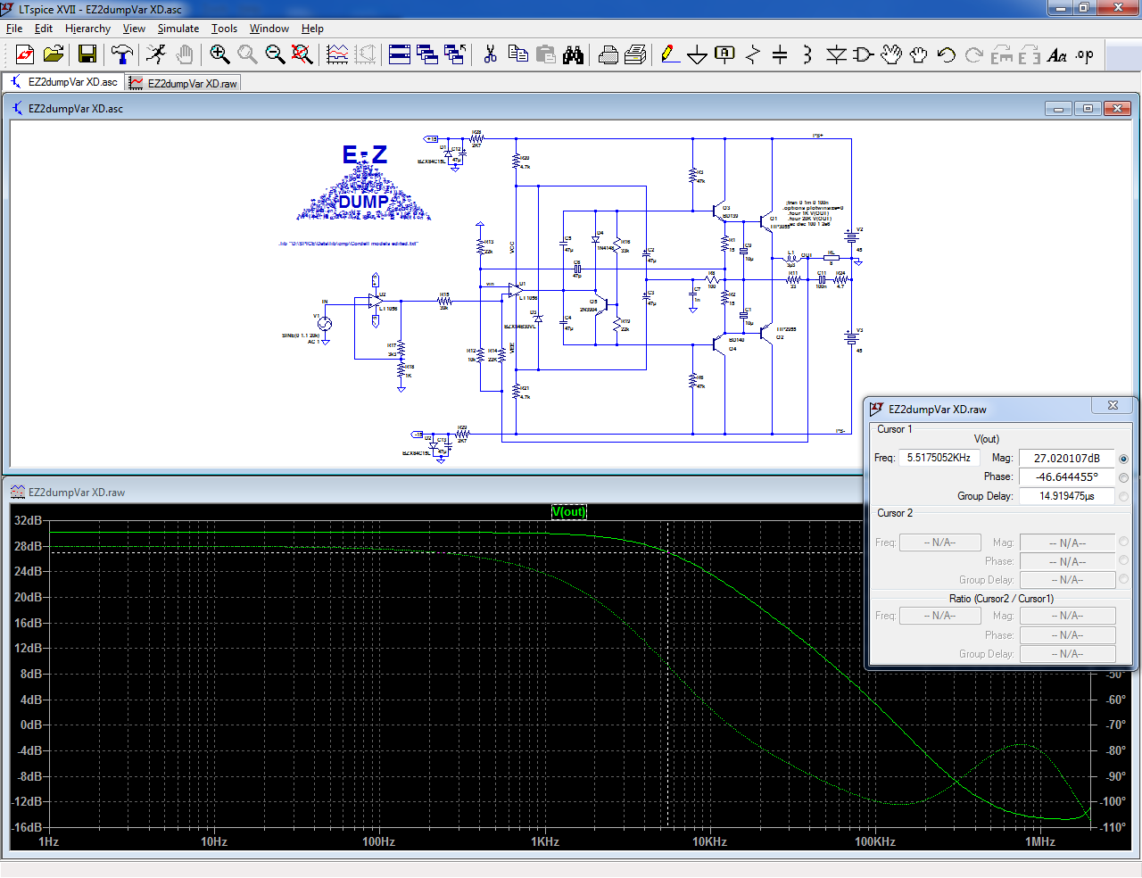
The difficult part of the circuit is the second stage: once it is stable in isolation, closing the global FB loop is a mere formality.
The overall stability is not really an issue, and needs not be conditional: the second stage operates in closed-loop, at a nominal gain of ~5 (it depends on the frequency and the amplitude), meaning the input stage operates at a gain of ~Gtot/5.
This is the gain plot of the second stage:
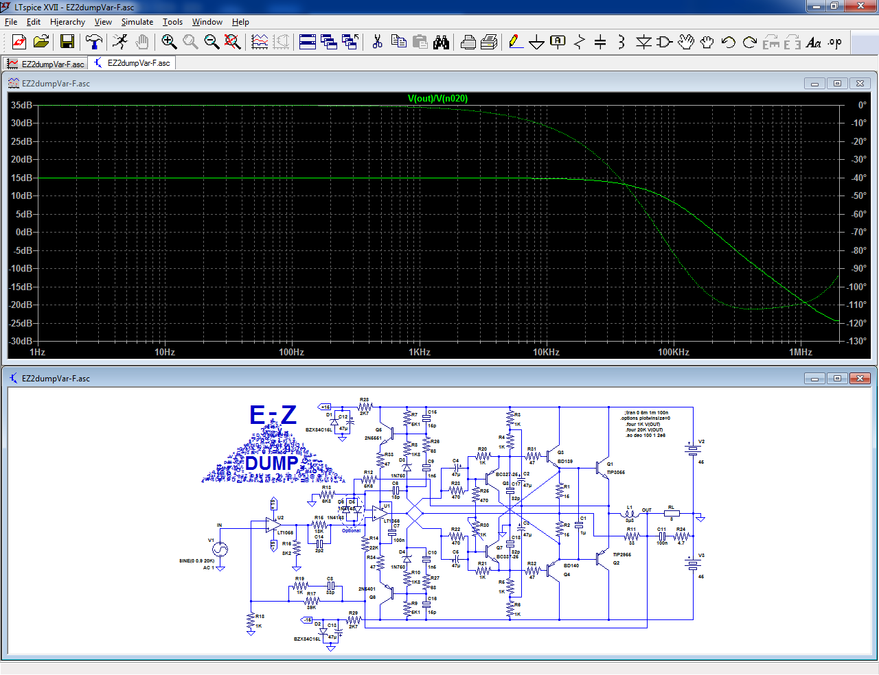
Since both amplifiers operate in controlled conditions, at a gain >1, they tolerate two stages + OP in the loop.
I finally managed to use a single bootstrap in reality:

It is not very docile though, and requires a small capacitor between the bootstrapped supplies and GND, C9.
The value of 33pF is quite critical: oscillations appear for C9<22pF or >47pF.
The instability is completely confined to the bootstrap: the wiring, base stoppers or shunt caps have no effect, and the outlook remains the same for a LF356, LF411 or TLO81.
The oscillations are identical with or without the input stage
The overall stability is not really an issue, and needs not be conditional: the second stage operates in closed-loop, at a nominal gain of ~5 (it depends on the frequency and the amplitude), meaning the input stage operates at a gain of ~Gtot/5.
This is the gain plot of the second stage:
Since both amplifiers operate in controlled conditions, at a gain >1, they tolerate two stages + OP in the loop.
I finally managed to use a single bootstrap in reality:
It is not very docile though, and requires a small capacitor between the bootstrapped supplies and GND, C9.
The value of 33pF is quite critical: oscillations appear for C9<22pF or >47pF.
The instability is completely confined to the bootstrap: the wiring, base stoppers or shunt caps have no effect, and the outlook remains the same for a LF356, LF411 or TLO81.
The oscillations are identical with or without the input stage
Attachments
I have tested many other opamp types for U1: OP15, OP27, etc.
The behavior remained more or less identical, except with a TL061: it didn't require the small C9 cap.
I think that a possible cause for the instability could be the capacitance between the bootstrapped opamp nodes and the ambient space: the whole bootstrapped circuit is "hot", and generates small capacitive currents into various pins, including the inputs but also the offset and frequency compensation.
Some kind of guarding would probably help.
You mean C14 (2p2) or C6 (18p) ?The behavior remained more or less identical, except with a TL061: it didn't require the small C9 cap.
No, sorry for the confusion: I mean C9 in the passive bootstrap attempt:

The final, active bootstrap version of post #63 seems to be more stable and less demanding.
It requires two additional transistors and wastes an additional 1~2V of output swing compared to the passive option, but it is probably safer if you commit to a PCB.
In the light of my latest findings with the passive bootstrap, it would probably be a good idea to include a shallow guarding of all the opamp pins, if it is still possible.
The guard doesn't need to be substantial: just a symbolic net of traces everywhere around U1, connected to its Vee or Vdd; a copper pour if you like, but there is no need to be that extreme: one just needs to interrupt the lines of the electrostatic field
Yes, version from post #63 is the one I'm going for.
I guess it's too late to add the guard, but there is plenty of Vxx traces going around U1 😀
I guess it's too late to add the guard, but there is plenty of Vxx traces going around U1 😀
- Home
- Amplifiers
- Solid State
- EZ-Dump: dump your current without really trying