Yes, I had lot of work, so there was not too much time for the amplifier.
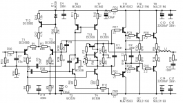
So here is the schematic, but I don't remember the values of the compensating network, due it was set during the measuring with scope. I use only the RC between the collectors of the input stage.
sajti
So here is the schematic, but I don't remember the values of the compensating network, due it was set during the measuring with scope. I use only the RC between the collectors of the input stage.
sajti
Attachments
MikeB said:Hi Chris, i also use a HP, i am not sure of the model, it's a networkprinter, it hink it's a HP5L...
Mike, you might want to give the following method a try:
Use artwork as viewed from the COMPONENT side. This way, when it is printed, the printed side will get in contact with the photosensitized PCB material, and there will be no gap due to paper or transparency thickness. The gap is responsible for difraction effects which limits the precision of artwork youc an use, even if it prints out correctly. Using this method I've done lines as thin as 8 mils (though you do need to correct somewhat n the artwork, i.e. make the lnes thicker by about 2 mil, since the photosensitive lacquer also has thickness and some diffraction).
Try printing on drafting cellulose transparency (pauspapier). The trick here is that it too has two sides, one slightly smother, though the difference is not great, and important only if you want to do truly thin lines. It also expands quite a bit when heated up. In the laser printer, teh heating and rolling through the rollers expoands it a lot in th elongitudinal direction. Whenever I get a new batrch of paper from a previously unknown maker, I 'calibrate' it by printing a long 'PCB' of known length on it, then measure and correct in the PCB program (most have correction factors for printing).
The trick to getting tru black comes in the form of acrylic protection lackuer. Not sure if and where it can be found outside Europe (I mean the one I use and know that it works), but Mike will surely know it: it's 'Plastic Spray' from Contact Chemie. What you do with it is the following: have it handy as well as a hair dryer. As soon as the transparency comes out of the printer, put it on a larger sheet of paper and spray it thinly with this 'Plastic Spray'. Count to about 10-15, then slowly dry it with the hair dryer (don't bake it, dry it holding the dryer about 30-50cm away). Don't ask me how I came up with that one, i don't remember 😉 but you will see that the spray sort of dissolves the toner slightly making it very black. It works best on lines that are relatively thin (where it's most important), but most laser printers do not deposit a whole lot of toner on the large black areas so only the outer edges of the areasw ill blacken completely. This is actually good as you will see in the next step. When the plastic spray has dried completely, turn over the artwork and repeat the procedure on the other side. What you get is toner that becomes a lot blacker, plus the tyransparency becomes more transparent - ideal! In addition, it acts as a sealant preventing warping due to moisture.
Finallr, get a good black marker and carefully retouch the large ares as these will not be completely black. Usually doing so on the back side of the artwork is enough, though best results are when done on both sides. Check for 'holes' against a window or something (ideally, a 'lighted table' such as used for checking photographs would be used.
Exposing works just fone using regular flourescent light (!), even the low power electronic bulbs will do fine, though the 'bluish white' nasty ones are actually the best. The best way I have found of doing this is to get a piece of glass (with rounded edges, you don't want t o cut yourself!), put the presensitized PCB copper up on a nice flat surface, then put the artwork print DOWN (in contact woth the copper) on the PCB and put t he glass on top. Typically it takes about 7-8 minutes from 25cm away woh a 11W fluorescent bulb mounted in a table light for me. I also have an exposure box built for the purpose, where the light source is in a ventilated box (uses a small fan), with a glass top surface, the glass is about 8mm thick and sits on small rubber spacers which enable the air to be sucked from the top edges of the glass and down into the box, and out the exhaust fan, to cool the 80W mercury bulb in there. Without the fan convection heats up the glass and PCB unacceptably. In this case, the artwork goes onto the glass, print up, the PCB goes on top of that copper down, and I normally put a big thick databook and a large surplus transformer on top of that to get really good contact between PCB and artwork. This is how I did the 8 mil line width PCBs...
I also calibrated the lighting process, by using a small piece of PCB and artwork with a set of lines and spaces drawn in parallel, with thickness from 30 mils down to about 10. I covered that with black paper and just kept moving it about a cm every half a minute to expose more and more of the artwork to light. When developed, check for best line and space rendition, and get the time from the distance on the PCB where it appears 😉
Developement is using NaOh. I don't use a pre-mixed solution as I have found there is quite a lot of tolerance from board to board. What I do is, i dissolve as many pellets of dessicated NaOh as I can in about half a liter of tap water, and put about a liter or so of tap water into the developing tub, and then put the exposed PCB in it. I add a little of teh concentrated solution at a time and stirr a lot, untill I can see the developing process start. Ittakes a bit of fine tuning to get it going perfectly. The idea is, in the end you have well over a liter of 'tuned' solution, which youc an store and re-use. It tends to work just fine untill teh solutiomn becomes almost the color of coke 😉, then you just use the remaining concentrate and repeat the process to get a new batch.
I do my etching with HCl (hydrochloric acid) and H2O2 (Hydrogen peroxide). Both are about 20-25% concentration and I use them because I can get them cheap - one is used for sanitary cleaning, the opther in swimming pools. Again, you start with just the acid and the PCB in it, and SLOWLY little by littel add the peroxide at the edge of the tub (NOT over the PCB!!!) and stirr profusely. At some point, you will start seeing very thin 'layers' of exposed copper washed away as you rock the tub making a 'wave' down the length of it and over the PCB. This is the perfect concentration. Beware that too much peroxide results in a rather spectaculairly quick etching solution, that also heats up and will destroy the PCB. Also, do this OUTSIDE, as you get chlorine gas as a result of the tching, DO NOT breathe in close to the tub! It is very corrosive and therefore dangerous. Fortunately it is heavyer than air and will stay on the ground. I've also done this in a semi-covered tub (tupperware 😉 ) in the bathtub, to keep the chlorine in there, after it is over, I just use the shower to precipitate the chlorine and wash it all down the drain. When the PCB is done, rince it profusely and also, a quick once-over with a little bit of soap (which is a slight ly) will neutralize the etchant.
I drill teh holes with the photoresist still on, as this protects the copper from being oxidated by fingertips. When I'm done, I put the board into the concentrated NaOh to strip off the photoresist, then it goes into VERY diluted hydrochloric acid (like a few drops of it in 1dl of water) and is dried, and immediately coated with solder varnish (flux dissolved in a spirit of some sort). It does not come off until everything is soldered on, at which ooint the board is cleaned from any soldering residue and that 'plastic spray' is sprayed over it to prevent corrosion.
Hi ilimzn !
Phew, what a great explanation ! Maybe you really should post that in the WIKI ?
Yes, i used the printed side down onto the copper, but i have not tried
yet the transparent paper ! And i did not know the trick with the "plastic spray"...
Need to try that !
I used the transparency-spray from Contact Chemie, this makes the
paper more/very transparent to UV-light.
Yes, for developing i also use NaOH, the trick is to find the correct
concentration...
The HCl and H2O2 is now getting difficult to buy, after the bombing
in London. I still have some left together with a 3rd chemical, but for
a very different purpose... Yes, i should be old enough to stop that... 😀
I use the Natriumperoxid as i can easily reuse it, i fill it into a bottle
and heat it up again when i need it again.
Important hint: open up the bottle once a week or so, to let out the gases...
And the FeClO3 is simply ugly...
I also keep the photoresist until i start soldering, but i used alcohol
and a toothbrush to clean it, the same i use for removing the flux
after soldering.
Big thanks for these informations, saved that on my harddisk !
What PCBs do you use ? I use Bungard-PCBs.
Mike
Phew, what a great explanation ! Maybe you really should post that in the WIKI ?
Yes, i used the printed side down onto the copper, but i have not tried
yet the transparent paper ! And i did not know the trick with the "plastic spray"...
Need to try that !
I used the transparency-spray from Contact Chemie, this makes the
paper more/very transparent to UV-light.
Yes, for developing i also use NaOH, the trick is to find the correct
concentration...
The HCl and H2O2 is now getting difficult to buy, after the bombing
in London. I still have some left together with a 3rd chemical, but for
a very different purpose...
Yes, i should be old enough to stop that... 😀I use the Natriumperoxid as i can easily reuse it, i fill it into a bottle
and heat it up again when i need it again.
Important hint: open up the bottle once a week or so, to let out the gases...
And the FeClO3 is simply ugly...
I also keep the photoresist until i start soldering, but i used alcohol
and a toothbrush to clean it, the same i use for removing the flux
after soldering.
Big thanks for these informations, saved that on my harddisk !
What PCBs do you use ? I use Bungard-PCBs.
Mike
A new Symasym was born
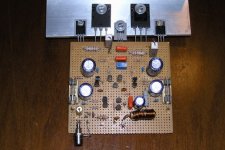
Symasym 5 prototype finished. One channel, parts were placed as in PCB and connected point to point. PS voltage is 2x32V. It worked flawlessly from the beginning. DC offset is 3.5 mV. Small transistors were matched with DMM. BC550C instead of MPSA18 at the input.
First impressions are very good, I will soon make PCBs for two channels.
Mr Mike Bittner, I think you should be proud about this amplifier🙂
Though I 'd like to have both channels with PCBs (and better capacitors and resistors) to make a more valid evaluation, I must say that from the beginning the most profound characteristics of this amp are dynamism and extraordinary detail in all frequences. I must also say that this is the first time that my speaker gave me correct, good, rythmic, controlled bass.
Minuses? Perhaps a little hard high frequnces? Or maybe I imagine things, or perhaps with all these ceramic capacitors all over and common resistors one cannot expect everything perfect 🙂
Have a nice day....
Attachments
Hi Dimitris,
welcome to the club ! And thanks for the compliments... 🙂
Nice to hear that it worked at once without problems and that you are pleased with the result !
About the harsh sounding, it shouldn't be, my latest version got rid of
any sign of harsh sounding. My latest changes were adding the 10ohms
between signalgnd and powergnd, the wire connecting the gndpins of
the supplycaps, and replacing the last ceramic-cap with a mica.
It's good possible that the use of ceramics cause harsh sounding.
The bc550c instead of the mpsa18 should not have big effect.
Are all components exactly the values from schematic ?
There is one thing i see on your photo and might be a problem, your
outputdevices ! What are they ? They are no MJLs, the right one looks
like a Toshiba, but the left one ??? I was wondering because of the
different packaging between npn and pnp...
Mike
Regarding harsh sound - I would suspect CD player or preamplifier (if used), the symasym amp might have discovered problem hidden by not so accurate amplifier before.
Re: A new Symasym was born
I would judge after having the proper PCB. Breadboard constructions may suffer from improper grounds etc. Also, 2 channels are needed to evaluate the sound ...
dtrif said:Symasym 5 prototype finished. One channel, parts were placed as in PCB and connected point to point.
I would judge after having the proper PCB. Breadboard constructions may suffer from improper grounds etc. Also, 2 channels are needed to evaluate the sound ...
Re: Re: A new Symasym was born
My PCB is the 2nd version. I have to modify the 1st, because of small hum, generated by the PSU. And this PCB contains all parts including the PSU capacitors, and the 4 output devices...
sajti
PMA said:
I would judge after having the proper PCB. Breadboard constructions may suffer from improper grounds etc. Also, 2 channels are needed to evaluate the sound ...
My PCB is the 2nd version. I have to modify the 1st, because of small hum, generated by the PSU. And this PCB contains all parts including the PSU capacitors, and the 4 output devices...
sajti
"the RL circut in the output need to be after the Zobel-circut!"
That usually seems to be the norm, but not for the Leach,why?
Is the diode connected transistor in the bias generator to modify the multiplication factor for an EF output, as per Doug Self's idea?
Brian.
That usually seems to be the norm, but not for the Leach,why?
Is the diode connected transistor in the bias generator to modify the multiplication factor for an EF output, as per Doug Self's idea?
Brian.
Re: Well...hehe.... never is too much late to learn new things.
hahahhhah
I listen your records in all day... Can you send more instructions? hahahha
Eu to escutando o que você me mandou todo dia... Você pode mandar mais intruções? É... hahhahaah... O esquema do ak... vai bem aqui... penso em postar ele aqui depois.... ihihihi I'm not a bad man....
Thanks!
destroyer X said:I have noticed that this kind of connection result noiseless related hum captured....but did not know those secondary problems that can happen.
I am 54 years old Pavel, and i thank you by your explanation, it is good that you are here with us, with this good will to give us informations about doubts we have...many other guys knows those details,but use to say that:
"Belf book, page 41, he used this approach to avoid capture of photonic energy from Andromeda"... well .... those things, that really do not turn things clear.
I think that hundreds will thank you, because there's a lot of things we do not know, and we go living ashamed to ask questions about that.
Great Mod Evil, you evoluted very fast....now you will turn my teacher, already elected for this job!...unless you are repeating what you have read perfectly memorized...ahahahaha!
regards,
Carlos
hahahhhah
I listen your records in all day... Can you send more instructions? hahahha
Eu to escutando o que você me mandou todo dia... Você pode mandar mais intruções? É... hahhahaah... O esquema do ak... vai bem aqui... penso em postar ele aqui depois.... ihihihi I'm not a bad man....
Thanks!
2SC 2526 bzw. 2SA 1076 als Endstufentransistoren ?
@ MikeB,
hallo MikeB,
was hällst Du von 2SC 2526 bzw. 2SA 1076 als Endstufentransistoren?
Siehe: http://pdf.alldatasheet.com/datasheet-pdf/view/61513/FUJITSU/2SC2526.html
und
http://pdf.alldatasheet.com/datasheet-pdf/view/87025/FUJITSU/2SA1075.html
Grüße aus Hessen
@ MikeB,
hallo MikeB,
was hällst Du von 2SC 2526 bzw. 2SA 1076 als Endstufentransistoren?
Siehe: http://pdf.alldatasheet.com/datasheet-pdf/view/61513/FUJITSU/2SC2526.html
und
http://pdf.alldatasheet.com/datasheet-pdf/view/87025/FUJITSU/2SA1075.html
Grüße aus Hessen
Hi dx.master !
You really should keep it english, it's an international forum...
These Fujitsu-devices do not look bad, especially the ft is impressive.
But, the vbe-curve is very weak, it's already 1v below 3A, the MJLs
have 1v at ~9A, also Vce-sat of 1v at 8A is not too good, the MJLs
have 0.25v at 8A. This might result in a weak, less powerful sound...
Regarding the powerhandling the Onsemi-devices seem unbeatable.
Just compare the SOA-charts for 10ms, the mjl3281 has 3.5a at 100v,
the Fujitsu only 1.2a...
About the sounding, i don't know !
Mike
Hi Mike
It is very very possible that the harsh sound is from the CD Player (Marantz CD-67SE) as PMA suggested, but I 'll have to build both channels on PCB to find out.
Mike, I am very pleased with the result (this harshnes is probably my fault and is very very small anyway to keep us talking about something so minor) and I am really going to build this amplifier as monoblocks, because I think it is in a class of its own, at least for me.
Yes, that may be one reason. I'll soon find out when I get rid of the ceramics!It's good possible that the use of ceramics cause harsh sounding.
Yes, all components except BC550C (instead of MPSA18) and output transistors are exact values.Are all components exactly the values from schematic ?
They are 2SC3281 (it is the same as MJL3281 I think, not sure though) and 2SA1943, because I had them handy.There is one thing i see on your photo and might be a problem, your outputdevices ! What are they ? They are no MJLs, the right one looks like a Toshiba, but the left one ???
It is very very possible that the harsh sound is from the CD Player (Marantz CD-67SE) as PMA suggested, but I 'll have to build both channels on PCB to find out.
Mike, I am very pleased with the result (this harshnes is probably my fault and is very very small anyway to keep us talking about something so minor) and I am really going to build this amplifier as monoblocks, because I think it is in a class of its own, at least for me.
For monoblocks, there is no need for that 10R resistor between IGND and GNDA, provided the VGND is not connected to Protective Earth.
Hi PMA,
Yes, it is highly possible for the CD player (Marantz CD67SE) to be the cause because I have some "hard" high frequences there, too, when I listen to it with good quality headphones. I don't know if this CD is known for such a kind of sound, though, or it is just my subjective perception that likes more "soft"sound.
I use a preamp, (DIY project) but the sound is more "harsh" without it, so it is probably not the cause.
Thanks for the interest.
Regarding harsh sound - I would suspect CD player or preamplifier (if used).
Yes, it is highly possible for the CD player (Marantz CD67SE) to be the cause because I have some "hard" high frequences there, too, when I listen to it with good quality headphones. I don't know if this CD is known for such a kind of sound, though, or it is just my subjective perception that likes more "soft"sound.
I use a preamp, (DIY project) but the sound is more "harsh" without it, so it is probably not the cause.
It is very possible, too.the symasym amp might have discovered problem hidden by not so accurate amplifier before.
You are absolutely right, it was not my intention to stick a label to the amp without having properly tested it, but to search for hints about what may be happening. Sorry if I was misunderstood.🙂I would judge after having the proper PCB. Breadboard constructions may suffer from improper grounds etc. Also, 2 channels are needed to evaluate the sound ...
Thanks for the interest.
Hi dtrif !
Yes, we will find out about the ceramics... 😀
Also for me, this cute amp is in a class of its own ! 🙂
About your outputdevices, the 2sc3281, have you bought it long time ago ?
I ask, because this transistor is obsolete, it is not manufactured since 2000,
so, all devices on the market with having a 2sc3281 printed on it are something else... 🙁
About the MJL, it should be quite similar to the 2sc3281, it was done by Motorola (now OnSemi)
to substitute the Toshibas some years ago.
The complementary to the 2sc3281 would be 2sa1302 (or 1304?), so your devices are very likely to be mismatched.
This could create problems, i don't know...
I suggest for a final version to get real complementary devices, you could use the sankens, the MJLs,
or the newer Toshibas ? (this 2sc5200) There are many good devices !
Mike
- Home
- Amplifiers
- Solid State
- Explendid amplifier designed by Michael Bittner, our MikeB