D
Deleted member 148505
Seriously? I had not implemented itin my current pcb, but as it takes less time to etch, I wanted to do this on my next print.
0.3mVac indicates a lot of noise on the amp output with a shorted input.
If I get that, I will try to find out what is wrong, not just an adjustment or two.
A really good amp will give noise (using specialist ultra low noise and precise band limiting amplifier and Voltmeter) of around 10uVac to 30uVac, 10Hz to 20kHz.
If I get that, I will try to find out what is wrong, not just an adjustment or two.
A really good amp will give noise (using specialist ultra low noise and precise band limiting amplifier and Voltmeter) of around 10uVac to 30uVac, 10Hz to 20kHz.
I like to allow for base stoppers. It is easy to short them out if not needed. 10r might be a bit high, but again these can be adjusted when provision has been made. I also like to see driver base stoppers.
Does reflect mean the same as capacitively couple? Or something else?................"Unconnected" ground pour is not advisable as it reflect signals to other areas...
D
Deleted member 148505
Does reflect mean the same as capacitively couple? Or something else?
I think of it more as an antenna that picks up noise from other signals and reflects it to other parts...
Ow, and I put the original gain-setting back which dropped the DC output from 30mV to 8mV, as it was before. Now find out why there is ac on the ouput and how to get rid of it.
What were the original resistor values attached to the +IN and -IN inputs?
What are the new resistor values?
These have a large bearing on the output offset.
The currents passing from the +IN and -IN inputs (the input bias currents) through the attached resistors generate the voltages at the +IN & -IN inputs. It's these voltages that flow through the amplifier to become the output offset.
You can play with the currents or with the resistances to change the offset and achieve a zero output offset at the operating temperature currently existing.
If you require a close to zero output offset tempco, then the input transistors should be accurately matched so that the offset currents remain matched over a wide range of operating temperatures.
No I kept the inut resistors according to the schematics. However, there is a resistor from the outpout to the voltage stage. I lowered that one from 22k to 11k. That worked well' but for some reason the measurements got worse. I had allready contacted mr. Elliott abut lowering the gain, but so far he had not contacted me.
We now know two of the eight resistors.
I'll assume that four of the unknown resistors are DC isolated from the inputs by DC blocking capacitors. I further assume that two match the original 22k.
I'll next assume that the input bias currents are 10uA, 2mA of Ic in each Q and an hFE ~200.
The voltage difference across the inputs with two 22k fitted would be zero (if all the other parameters are perfectly matched). With a 22k and an 11k the Vdiff becomes [22k-11k] * 10uA = 110mVdc
Changing one resistor from 22k to 11k, with the assumptions I have chosen, will change the output offset by 110mVdc.
Last edited:
Pff, new day, new chances. Shorted the input, measured AC and now I get a 0.0 mVac sometimes going to 0.1mVac. DC offset around 4 mVdc. Maybe it's time to put the amp aside for a couple of days and rethink the layout and measurement methods.
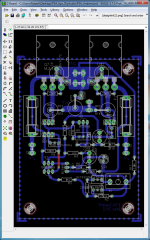
The current layout is attached below.
The current layout is attached below.
Attachments
D
Deleted member 148505
I'm sorry to butt in here guys. I'm also trying to make a layout, can you comment on these, which one is better? thanks
You can download and try the first one here
You can download and try the first one here
An externally hosted image should be here but it was not working when we last tested it.
An externally hosted image should be here but it was not working when we last tested it.
Last edited by a moderator:
If I understand the comments made earlier correctly, it is advised to split the powergnd and signalgnd.
But if I recall correctly, you had already made a channel right? If so, why not try to measure some sort of performance?
But if I recall correctly, you had already made a channel right? If so, why not try to measure some sort of performance?
may one address the subject to a moderator and out of the blue we will have
Today's P3A pcb contest !!!😛😀😛😀
I prefer the layout of Jlester 87
kind regards
sakis
Today's P3A pcb contest !!!😛😀😛😀
I prefer the layout of Jlester 87
kind regards
sakis
D
Deleted member 148505
If I understand the comments made earlier correctly, it is advised to split the powergnd and signalgnd.
But if I recall correctly, you had already made a channel right? If so, why not try to measure some sort of performance?
I didn't split the power gnd and signal gnd because it requires major changes to my current layout so I have to make compromises to the design.
Also, I can't measure the performance because I don't have proper equipment(s) to do so, and I don't have an oscilloscope here to check for oscillations, that's why I'm posting my layout here so that anyone can try and check the layout's performance. (I'll remove it soon, for respect to rod elliot)
Your layout is also good, I won't be surprised if it performs better than mine...
Nope, I used to126/sot32 package, so that q9 can be (easily) thermally coupled with the driver tranniesIs Q9 a BC546 in your schematic jlester87?
may one address the subject to a moderator and out of the blue we will have
Today's P3A pcb contest !!!😛😀😛😀
I prefer the layout of Jlester 87
kind regards
sakis
Oh no, that's what I'm trying to avoid here, maybe I'll just delete my previous comments and put it in another thread... 🙂
Although my layout was based from alexmm's p3a design layout, I find this thread full of ideas so I integrated some of your suggestions to his layout.
Last edited by a moderator:
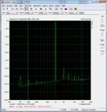
Take one torroid, 2 caps, 4 diodes and you get a better measurement than with a 400 dollar power supply.... I cheated a bit by using an iPhones battery operated signal generator, but when I used the iPhone with the labsupply I got 50-500 Hz noise, with the simple torroid that's less.
THD+N is around 0.012% at 1.6 Watt (3.9 Vac over 9.4 Ohm)
Update;
And adding 2*10 mF caps damped the 100 Hz peak by over 5 dB and 50 Hz by 4 dB. We are making progress. 4 days the output looked like http://www.diyaudio.com/forums/solid-state/212342-esp-p3a-layout-4.html#post3040762
THD+N is around 0.012% at 1.6 Watt (3.9 Vac over 9.4 Ohm)
Update;
And adding 2*10 mF caps damped the 100 Hz peak by over 5 dB and 50 Hz by 4 dB. We are making progress. 4 days the output looked like http://www.diyaudio.com/forums/solid-state/212342-esp-p3a-layout-4.html#post3040762
Attachments
Last edited:
- Status
- Not open for further replies.
- Home
- Amplifiers
- Solid State
- ESP P3A Layout