Some of the people here are not EEs.
Then why the pun below? Do you realize you are insulting people you have no clue about their expertise? What about instead something like "OPA1611 comes close to an ideal op amp for the IV stage, because...". That would be both constructive and helpful to those non EEs; as a plus, I would have no reason to comment.
InspectorGadget,
All that stuff has been discussed in this thread before. Many folks at some point focus their thinking on choosing opamps, and on calculating stuff they know how to calculate.
That day you are waiting for isn't going to happen until I can get AK4499 again, or else an acceptable substitute for music reproduction. In other words, not an ESS part.
How convenient, isn't it?
I keep telling people about OPA1611/OPA612, but a lot of them are intent on trying other opamps. I guess some people just have to find out for themselves. What concerns me more is when more experienced people come along and start suggesting opamps to newbies who are not equipped to evaluate them in circuits, maybe except by FFT comparisons using ADCs full of spurs. No notch filter and makeup gain to get around the ADC spurs. Far from ideal. All I can do is try. (Besides, IMHO typical audio FFTs don't tell the whole story)
Last edited:
What concerns me more is when more experienced people come along and start suggesting opamps to newbies who are not equipped to evaluate them in circuits, maybe except by FFT comparisons using ADCs full of spurs. No notch filter and makeup gain to get around the ADC spurs.
What do you think of the second incarnation of the notch filter shown in this link? The incarnation with the film capacitors? (Not the first one with the ceramic C0G capacitors.) Quick and Simple Notch Filter for THD Measurements – Toli's DIY
It looks like a fairly easy but quite valuable project.
Hall filters are good. Component matching matters for a deep notch. Ideally, its good to drive it with a low impedance and load it with a very high impedance. OPA1611 make good input and output buffers.
The particular notch filter you linked to shows has some FR graphs. You can see that there is considerable attenuation over the first few harmonics, which isn't great.
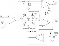
Myself, I use an active Hall notch filter. It can be tuned to level out the response by the 2nd harmonic (at which point the notch is 38dB deep), and it has the usually needed I/O buffering. Schematic attached below. My construction uses a ground plane. I made it so I can use plugin tuning modules preset for different frequencies. That is, the modules have the actual RC filter components on it. Instead of the bandpass output, I used the spare half of an OPA1612 for 10x of makeup gain at the output. The output to the ADC can be taken before or after the 10x gain stage.
The particular notch filter you linked to shows has some FR graphs. You can see that there is considerable attenuation over the first few harmonics, which isn't great.
Myself, I use an active Hall notch filter. It can be tuned to level out the response by the 2nd harmonic (at which point the notch is 38dB deep), and it has the usually needed I/O buffering. Schematic attached below. My construction uses a ground plane. I made it so I can use plugin tuning modules preset for different frequencies. That is, the modules have the actual RC filter components on it. Instead of the bandpass output, I used the spare half of an OPA1612 for 10x of makeup gain at the output. The output to the ADC can be taken before or after the 10x gain stage.
Attachments
Last edited:
Would you recommend an active Hall notch filter over an active Twin-T notch filter such as described here? Active Twin-T notch filter
Twin-T is good too. IIRC it can give a very deep notch, but they can be harder to tune than the Hall filter I showed. The schematic you linked to shows 3-variale resistors. In reality, even if they were 25-turn trim pots they would probably be too hard to adjust finely enough for what you would need to optimize the notch depth and notch frequency at the same time. For each resistor on the schematic, you might need to use a fixed resistor in series with a low value 25-turn pot so you could narrow in on the null without always overshooting it, while at the same time keeping the frequency of the notch where you want it. Also something to be aware of, pots themselves can add some distortion. The resistor elements inside and the wipers have some nonlinearity. If you use good quality trim-pots and good metal film resistors I think you would probably be okay for your purposes.
EDIT: Regarding the overall project shown in the link you gave, while it may give a deep notch I have doubts it is carefully enough designed and built to be clean enough for you to clearly distinguish dac spurs down at -130dB or lower. The reason that matters when working with dac chips like ES9038Q2M is because it is possible with very careful dac design to get all the HD spurs down that low. You may find you need to if you want to hit that -120dB overall distortion spec of the chip.
EDIT: Regarding the overall project shown in the link you gave, while it may give a deep notch I have doubts it is carefully enough designed and built to be clean enough for you to clearly distinguish dac spurs down at -130dB or lower. The reason that matters when working with dac chips like ES9038Q2M is because it is possible with very careful dac design to get all the HD spurs down that low. You may find you need to if you want to hit that -120dB overall distortion spec of the chip.
Last edited:
Hall filters are good. Component matching matters for a deep notch. Ideally, its good to drive it with a low impedance and load it with a very high impedance. OPA1611 make good input and output buffers.
The particular notch filter you linked to shows has some FR graphs. You can see that there is considerable attenuation over the first few harmonics, which isn't great.
Myself, I use an active Hall notch filter. It can be tuned to level out the response by the 2nd harmonic (at which point the notch is 38dB deep), and it has the usually needed I/O buffering. Schematic attached below. My construction uses a ground plane. I made it so I can use plugin tuning modules preset for different frequencies. That is, the modules have the actual RC filter components on it. Instead of the bandpass output, I used the spare half of an OPA1612 for 10x of makeup gain at the output. The output to the ADC can be taken before or after the 10x gain stage.
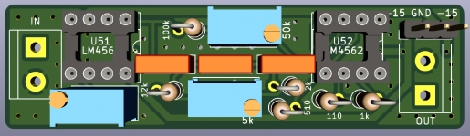
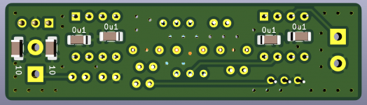
I have attached an early rough draft of an active Hall notch filter. Ground is poured on top and bottom with vias to connect more isolated portions.
Any suggestions to improve it? R57 is to prevent oscillation. I decided to keep blocking caps in the DUT as well as the sound interface.
The LM4562NA bypass capacitors are 0.1uF X7R and 10uF X5R.
Attachments

Last edited:
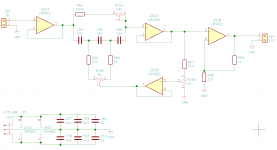
Filter looks pretty good at first pass. One warning though, I couldn't tune the notch depth in mine using the basic schematic because the adjustment was too sensitive. I kept overshooting the null. So I added a small pot in series with 5k pot and reduced the 12k resistor by half the extra pot's resistance. I did that by putting a resistor in parallel with the 12k. Then adjusted the extra pot to midpoint and tried again to null with the depth pot. When I started overshooting the notch null, I got it as close as I could then slightly tweaked the extra pot to get a bit of fine tuning. It worked okay. Still got the same null depth everyone else gets. Might have been my 5k trimpot was 10-turn rather than 25-turn, don't remember now. Also, I think I might prefer electrolytic 10uf caps rather than ceramic. Maybe consider Panasonic FM series, lowest value in that line is 22uf. IME those caps can take some time to fully 'break in' but I like 'em a lot once they do. Suggest not to be taken in by famous cap names and try some good cheap ones.
EDIT: Bourns 3296 trim pots are 25-turn cermet which are pretty good, lot of people use them. https://www.bourns.com/docs/technic...lications/bourns_trimpot_catalog.pdf?sfvrsn=0
EDIT: Bourns 3296 trim pots are 25-turn cermet which are pretty good, lot of people use them. https://www.bourns.com/docs/technic...lications/bourns_trimpot_catalog.pdf?sfvrsn=0
Last edited:
I have read Cyril Bateman's work (such as on the SU bipolar series) and as a result I have some Panasonic capacitors already. I have also done some capacitor distortion measurements and I recently paralleled a number low distortion op-amps to enable extension of my measurements.
I also plan to get more Panasonic SU series as I suspect the dual thick oxide capacitors are quite good.
I also plan to get more Panasonic SU series as I suspect the dual thick oxide capacitors are quite good.
I don't know if this is a good or bad idea but I might try adjusting on a first pass and then replacing the 1% resistors with the closest resistor + potentiometer setting value, then replace the potentiometers with lower values (perhaps 1/5 or 1/10 of the initial value) and then fine tuning. A little messy but might be better and more stable long term.
About swapping resistors, I get a 100-ohm or 200-ohm trim pot. If I set the 100-ohm one to midpoint I nominal 50-ohm resistor. On the other hand, if I swap fixed resistors I can only get them in whatever the standard increments are. That may or may not be close enough to solve a fine tuning problem. Of course, you can do some analysis and estimate whether it seems likely to work or not. It might be fine.
If you aim to draw 4-layer PCB for this Dac, how should the 4 plane be?
1: Digital signal and analog out? 2: gnd? 3: power? 4:gnd?
BR // Daniel
1: Digital signal and analog out? 2: gnd? 3: power? 4:gnd?
BR // Daniel
Hi Daniel,
Probably its wise to plan out what you want to do before going to far with assigning layers. We can make some initial good guesses though:
1. Signal traces and ground fill areas.
2. Ground plane or large ground fill area (depends what design rules you want to have apply).
For layers 3, 4, I would say it depends on your plans. It might make sense to put +5v bus power in a fill area on layer 3 around and under the dac chip/RF/digital area of a dac board.
If planning on local regulators for DVCC, VCCA, and clock, and maybe for MCU just to keep it off other rails, then I would ask where are you planning to put the regulators? On layer 4, the bottom? On top, but make the board bigger so there is more area for regulators there? Depending on what your plans are you might want to put regulators on the bottom, layer 4. In that case it might look a lot like layer 1, various signal and control signal traces and an area of ground fill.
Maybe closer to other end of the board, call it the analog audio end, the layer 2 ground plane/fill should probably be a continuation of that under the dac chip. Layer 1 might be signals and local ground fill dedicated to the analog audio section of the board. Layer 3 might be an opamp Vcc- rail fill area, and layer 4 a Vcc+ fill area (I put them in that order since I might want to neg rail to have more ground capacitance to layer 2 to help stabilize it since that is the reference rail for most opamps).
Anyway, the main point is that when designing a dac board I probably wouldn't start drawing a schematic in the PCB design program. Rather I would start with pencil, paper, and a big eraser, to draw maybe a system diagram, a schematic, and a rough layout plan thinking about signal routing and signal flow. For example, I never understood why in your analog output stage board you laid out the opamps at 90-degrees to the way I would have done it. For a dual opamp, pins 1 and 7 are the non-inverting inputs so point them towards where the input signals are coming from, the dac chip. Pins 3 and 5 are the outputs so point them to where the signals are going next, to the dac board outputs to maybe to a differential summing stage.
Regarding selection and mounting of components, the dac chip has a ground pad so it will need to be 'cooked' on in a reflow oven or by other field expedient means. Good to use SMD bypass caps for most things, although for clock and I/V opamps I might use 805 SMD film. I might want to try OPA1656 in addition to OPA1612 just to see how the two most likely seeming candidates compare (could be OPA1656 will turn out to be more tolerant of RF going into the input pair, don't know if it would be an overall improvement though). If you decide to do a differential summing stage maybe we should talk about that separately. Hopefully by the time the dac output signals get there you might be able to get away with through hole film caps for bypass since a lot of the highest frequency RF would ideally be attenuated enough.
Another thing to think about before you start designing a board is whether you will allow an option for SMD or though hole parts in certain places. For whatever you want to do you should think about good layout, and also choose components you want to use and start collecting footprint patterns to prepare you design library. Once you really know what you want to do, then enter the schematic and component choices in the PCB design program, and then layout as best you can according to your already well considered plan.
EDIT: We should also talk some more if you think you might want to do a synchronous clock design, or maybe leave an option to do it.
Last edited:
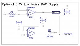
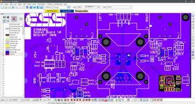
I have just downloaded the es9038q2m evaluation board layout file and it doesn't look good at all to me:
AGND_L have no short way to connect to output gnd, it will take long way either through right channel ground or through power supply ground which is not good at all to me.
The gerber file also have a layer call board which seem like either a solid ground plane ( which is good for performance) or just to indicate board dimension (more likely this case because if it's a physical layer then this board has only 3 layers).
The design file can be download here: https://ismosys.com/wp-content/uploads/2020/08/ES9038Q2M-Ver-1.0.zip
what current is going to be flowing in output ground if you are using balanced outputs? there is no 3rd layer. its a 2 layer board. ground fill is separated into DGND and AGND with a keepout, but copper pour is filled with AGND in top part of the board and DGND on bottom, with just keepout/guard separating them. neither AGND or AGND left has totally direct return from output GND, both flow through a via to the GND fill and both are tied together. or you are referring to feedback ground? same case for that. I do agree though; its not ideal ...
Last edited:
Its just an evaluation board, not the best nor the worst possible implementation. Presumably it can at least produce the claimed specifications printed in the data sheet. ESS don't make any claims that it will sound good, although they do sometimes like to point out that the noise-shaper doesn't produce very much noise floor modulation. IME, getting the dac to sound its best is not so simple.
Attachments
Last edited:
Its just an evaluation board, not the best nor the worst possible implementation. Presumably it can at least produce the claimed specifications printed in the data sheet. ESS don't make any claims that it will sound good, although they do sometimes like to point out that the noise-shaper doesn't produce very much noise floor modulation. IME, getting the dac to sound its best is not so simple.
If it can produce specification in datasheet, it must be at least a good implement.
what current is going to be flowing in output ground if you are using balanced outputs? there is no 3rd layer. its a 2 layer board. ground fill is separated into DGND and AGND with a keepout, but copper pour is filled with AGND in top part of the board and DGND on bottom, with just keepout/guard separating them. neither AGND or AGND left has totally direct return from output GND, both flow through a via to the GND fill and both are tied together. or you are referring to feedback ground? same case for that. I do agree though; its not ideal ...
Yes, you're correct, i forget that this is a balanced board. The es9018k2m eval board which have se output have clear path form output gnd to agnd. But it still have some problem like decoupling cap for AVCC is too far, it must be about 2 cm from the cap to chip pin.
- Home
- Source & Line
- Digital Line Level
- ES9038Q2M Board