Stm32f446 datasheet give following values as jitter:
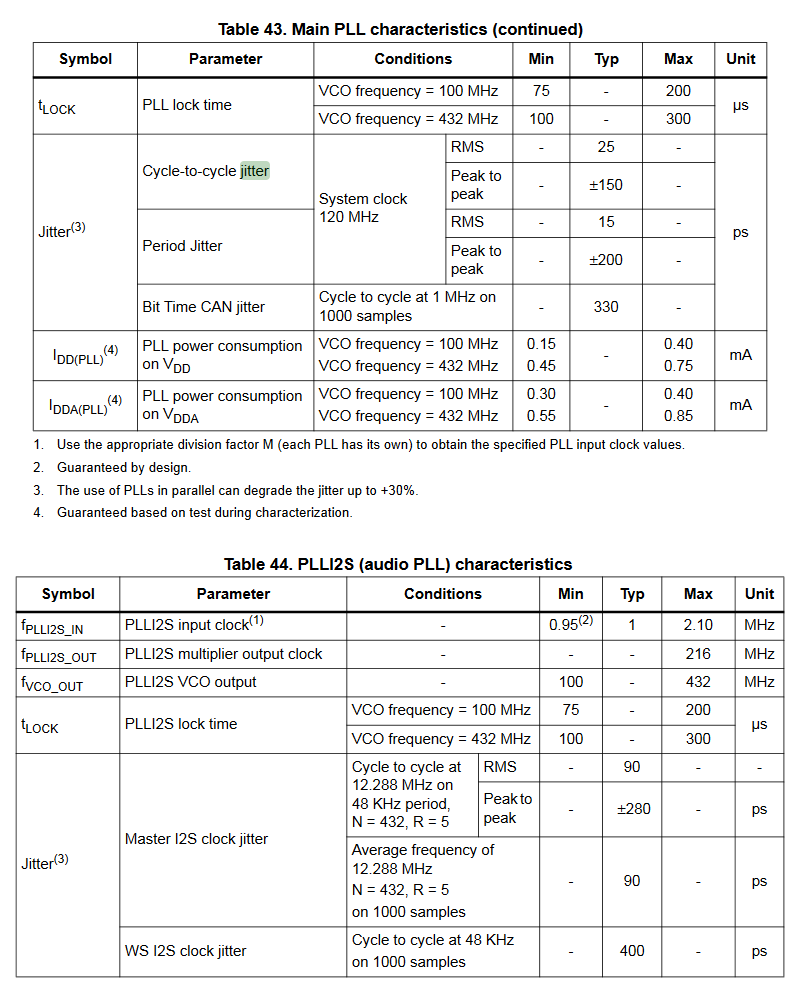
I'm surprised PLLI2S have more jitter than Main PLL, anyway even +/-280ps jitter is a high value ? I mean this is measurable in terms of THD ? (I think jitter affect mainly THD, maybe I'm wrong). It's something I can measure (I own a QA403), THD versus ASRC or not, different clock frequency etc... one time I build this pcba. Note: I will add footprint for a 100Mhz low jitter oscillator in my design as a option, in such way can measure correctly affect of jitter.
As a lower noisy LDO I can use LM5907, cheap, good availlability and indeed a /10 noise compared to TLV755.
JensH, how thanks, didn't see this mistake!
Some SPDIF receivers have lower jitter. Not saying it's audible but with dedicated audio clocks you could have much lower jitter.
LP5907 is much better than TLV755 but LT3042 or TPS7A94 would be even better.
LP5907 is much better than TLV755 but LT3042 or TPS7A94 would be even better.
Indeed I see some picture of high end audio device, it's beautifull but not my wishes. Certainly cause by my professional life where a smart design is a easily manufacturable, testable, made of available parts for medium size production. Audio works should be fun for me, and I get the fun with a design looking smart for my opinion 🙂 Also I try to run fast, cause I've a power amplifier pcba who wait for his dac.
Parts you suggest, LT3042/TPS7A94 show a noise improvement about 10 times compared to LP5907, the price follow this improvement 10x times higher, and complexity also (10 pins package, feedback, single sourcing regarding pinout...). My last professional design was about an ADC analog front end with some analog process and the usage of such very low noise ldo is a good choice for that (we need 20bits enob with a 5V single rail), I prefer using low noise OPA as LDO to achieve noise perfomance because it's cheaper and multi source.
I doubt using such high end ldo for this dac is pertinent, I doubt if even I can measure noise difference. On other side using LP5907 instead of TLV755 worth it, and thanks for that.
Off course I fully understand the pleasure of using only high end parts, no compromize, best performance, this is simply not my taste.
About jitter, it will be interesting to measure THD with a high jitter (high here is above 100ps, below 1ns as I understand) and a low jitter clock, sourcing the dac.
The most expensive clock I quickly found on mouser, about 30$:
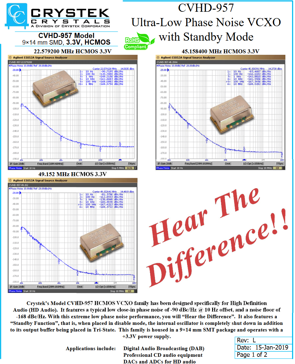
Indeed, better way to Hear because measure will cost you a laboratory instrument that cost a nice car 🙂 That's my opinion, will be happy to change it and learn why 🙂
Parts you suggest, LT3042/TPS7A94 show a noise improvement about 10 times compared to LP5907, the price follow this improvement 10x times higher, and complexity also (10 pins package, feedback, single sourcing regarding pinout...). My last professional design was about an ADC analog front end with some analog process and the usage of such very low noise ldo is a good choice for that (we need 20bits enob with a 5V single rail), I prefer using low noise OPA as LDO to achieve noise perfomance because it's cheaper and multi source.
I doubt using such high end ldo for this dac is pertinent, I doubt if even I can measure noise difference. On other side using LP5907 instead of TLV755 worth it, and thanks for that.
Off course I fully understand the pleasure of using only high end parts, no compromize, best performance, this is simply not my taste.
About jitter, it will be interesting to measure THD with a high jitter (high here is above 100ps, below 1ns as I understand) and a low jitter clock, sourcing the dac.
The most expensive clock I quickly found on mouser, about 30$:
Indeed, better way to Hear because measure will cost you a laboratory instrument that cost a nice car 🙂 That's my opinion, will be happy to change it and learn why 🙂
You can get NZ2520SDA with better performance for 10x less.
https://www.digikey.fi/en/products/filter/oscillators/172?s=N4IgTCBcDaIHYC8wFYwAYDOATAhiAugL5A
But both NZ2520SDA and CVHD-957 are pointless if you use them as a source to PLL.
https://www.digikey.fi/en/products/filter/oscillators/172?s=N4IgTCBcDaIHYC8wFYwAYDOATAhiAugL5A
But both NZ2520SDA and CVHD-957 are pointless if you use them as a source to PLL.
Maybe try: https://www.diyinhk.com/shop/audio-...frequency-451584mhz/113-magnifier_option-nullAlso will take a look on NDK SDA series...
Regarding Crystek, IMHO and IME they sound best with a carefully designed power supply, and with Rubycon 805 SMD film, .22uf bypass caps (which are not cheap either). Also I personally would not use ferrite beads, although nothing wrong with putting a pad for a bead in case it turns out to be needed. Could always put zero ohm resistor on the pads if the ferrite isn't needed.
EDIT: Regarding LDOs for AVCC, I am not fan of the sound of some of them. LT3042/5 and ADM7150 are ones that didn't sound good to me, but it did get better with ADM7150 when I loaded it down with a resistor to ground. That gets more current flowing through the pass transistor, which may have the effect if increasing loop gain of the error amp.
Last edited:
Hi, almost finish layout of my es9038 board 🙂 This board is purposed to fit my amp, so there are specific connectors for analog/power and other thing relative to my amps. Will order soon@jlcpcb to start manufacturing 🙂
This board embed a STM32F446 as a USB streamer (using UAC2 open project https://github.com/slerpxcq/openuac2_fw) and main general controler. There is also a Bluetooth module (chinese one Muyu or Feasycom).
I add a clean jitter clock option to see if I can measure/hear the difference compared to initial plan using STM32 pll.
Here the file of kicad project (v7 not yet going on 8).
Off course will keep you updated on board bring bring up 🙂
Attachments
Still not right. AVCC at the dac chip is supposed to 3.3v. Not half of that. AVCC/2 is only for the I/V opamp noninverting input.
Also, I have attached your schematic as a PDF. You need to make it easy for people to look at your design. They shouldn't be forced to open it in KiCad.
Also, I have attached your schematic as a PDF. You need to make it easy for people to look at your design. They shouldn't be forced to open it in KiCad.
Attachments
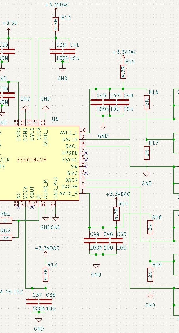
I guess you speak about resistors R15&R14, looks on value it's only to add a small decoupling between both AVCC_x pin. AVCC/2 for opamp are made with other resistors R16/R17.
And you right, thanks sharing PDF, I share kicad file to simplify work for those who wants to do their own implementation.
And you right, thanks sharing PDF, I share kicad file to simplify work for those who wants to do their own implementation.
Looking at it again, you're only using RC filtering on the noisy +3.3v dac, and it making a small part of a voltage divider with R18, and R19.
The dac will play audio that way, but unlikely it going to meet specs for what chip is capable of. The sound will be distorted with noise, etc. Using a bunch of different value caps in parallel is usually considered a bad idea nowadays too. It can make the impedance vary wildly with frequency because each cap as parasitic inductance and self resonance. One cap's capacitance can resonate with another cap's inductance to create problems.
Better to dedicate a low noise, nice sounding 3.3v regulator for each AVCC pin. If you don't want to do then you probably picked the wrong dac chip. You want a easy chip, not a demanding one.
Hi, you sugest something like this ?
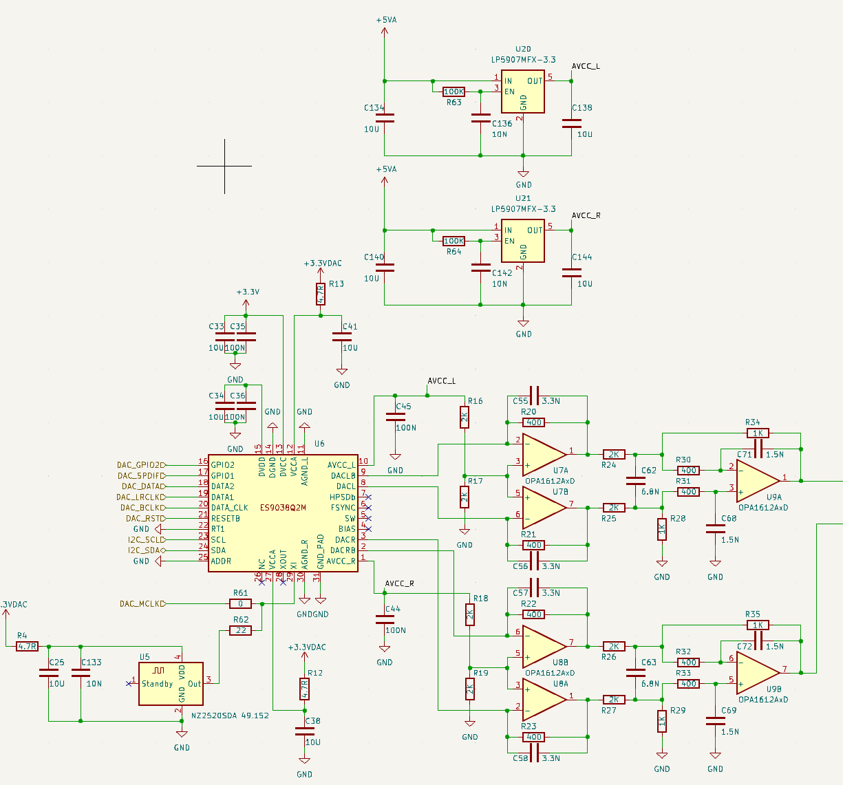
Now three low noise LDO, one vor VCCA portion of the IC, and one for each L/R analog circuitry.
I remove small 100nF caps of analog part, except for digital side, I often use bunch of differents caps in digital design to make a power distribution network with small impedance in frequency of interest, but that's more relative to high speed design than low noise analog.
I'm here to learn then will follow your experience, and thanks for that 🙂
I also use bunch of caps for opamps:
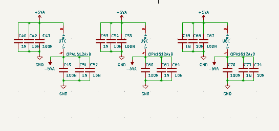
Better way to only keep one of 100nF for each opamp power pin (and eventually biger value than 100nF) ?
I just open my QA403 audio analyser to watch about hom they manage es9038 inside, looks like there is one ldo for each AVCC_x port 🙂 also opamps use only one caps for each power pin.
Now three low noise LDO, one vor VCCA portion of the IC, and one for each L/R analog circuitry.
I remove small 100nF caps of analog part, except for digital side, I often use bunch of differents caps in digital design to make a power distribution network with small impedance in frequency of interest, but that's more relative to high speed design than low noise analog.
I'm here to learn then will follow your experience, and thanks for that 🙂
I also use bunch of caps for opamps:
Better way to only keep one of 100nF for each opamp power pin (and eventually biger value than 100nF) ?
I just open my QA403 audio analyser to watch about hom they manage es9038 inside, looks like there is one ldo for each AVCC_x port 🙂 also opamps use only one caps for each power pin.
Better. One thing you could do is strongly filter one AVCC voltage regulator output, then buffer that with a unity gain non-inverting OPA1612 powered from clean +15v and GND in order to produce two buffered AVCC output voltages for the dac AVCC inputs. There are other things you can do too, maybe someone else will suggest something.
Out of curiosity why use the ES9038 (Hyperstream II) versus the new ES9039 (Hyperstream IV)?
https://www.mouser.com/ProductDetail/ESS-Technology/ES9039Q2M?qs=OcgtsXO%2B3gsGISPYpHXYiA==
https://www.mouser.com/ProductDetail/ESS-Technology/ES9039Q2M?qs=OcgtsXO%2B3gsGISPYpHXYiA==
Mainly because I will find more easily exemple of es9038 programmation/configuration. As es9039 is brand new there is less exemple with it.
Also my objective is to build a 'simple' digital board for one of my power amp, I will not search for last ppm thd and noise below 50µVrms will be large enought for my amp.
Also my objective is to build a 'simple' digital board for one of my power amp, I will not search for last ppm thd and noise below 50µVrms will be large enought for my amp.
I don't suggest it for the last PPM in distortion. More of a suggestion from others who say that Hyperstream IV has a more natural sound than Hyperstream II. Over the years I have read a number of criticisms of the sound of ESS even thought they exhibit very good THD and SNR measurements. AKM was suggested as having a better sound. I don't know the reasons for this but often I wonder if it has something to do with conversions and filtering. Anyways I thought I would suggest it since some seem to think that ESS has improved with Hyperstream IV. Eventually I would like to compare a good implementation of the latest AKM to a good implementation of Hyperstream IV. I don't put too much stock into the last PPM in distortion as there are plenty of bad sounding implementations that could otherwise perform much better. The board this thread talks about is a pretty good example of a bad implementation, for example.
hmm, sounds like arguments who can hits 🙂 I just start to understand how works es9038 and read that configuring it is not easy easy... other way 39 has hw config which is typically a good point for hw guy like me. I starts my design with a ak4490 dac, and move to es for spdif input and src engine inside chip. I initialy take a look on 39 datasheet but don't find out how it works (no deep reading of datasheet). For 38 I understand easily the relations between clock input and possibilities of FS when src on or off. Maybe the same in 39 I maybe miss something in the datasheet... Need urgently to wait for more reflexion 🙂
Have built with 38 and 39 (PRO). S.Q is significant better in 39.
And as you say, if you dont want to use a MCU it’s possible to just use HW.
And as you say, if you dont want to use a MCU it’s possible to just use HW.
Another point to modify my design replacing 38 for 39 🙂
Maybe I can ask you how to manage the 39? I speak about I/V stage, it's a good idea to use such schematic?:
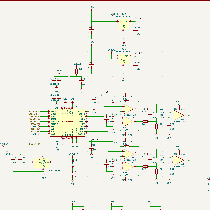
I will also have difficulties in understanding how manage clock with 39;
Plan for 38 was to feed dack with 44.1 or 48k clock when using in I2S depending on I2S FS stream, in a synchronous way. For SPDIF plan was to feed 38 only with a 48k family clock and use ASRC and DPLL to generate good 44.1k (when SPDIF stream is 44.1) family using the 38 datasheet formula:

Is this plan compliant with 39 ?
Maybe I can ask you how to manage the 39? I speak about I/V stage, it's a good idea to use such schematic?:
I will also have difficulties in understanding how manage clock with 39;
Plan for 38 was to feed dack with 44.1 or 48k clock when using in I2S depending on I2S FS stream, in a synchronous way. For SPDIF plan was to feed 38 only with a 48k family clock and use ASRC and DPLL to generate good 44.1k (when SPDIF stream is 44.1) family using the 38 datasheet formula:
Is this plan compliant with 39 ?
DPLL number (register 66-69) is read only information for calculation of actual sample rate. It may be better to use non-audio clock frequency for ASRC (e.g. 50MHz).
If using 50Mhz for exemple can achieve 44099.998hz for 44.1 and 48000,004Hz for 48k now if i use a audio clock 49152000 48k will be 48k but 44.1k will be 44100.0023. As a newbi using an audio clock looks best cause you have at least one fs family perfect and the other near perfect, using 50M you get both near perfect. It's not that caracteristic you speak about when you sugest using non audio clock ?
- Home
- Source & Line
- Digital Line Level
- ES9038Q2M Board