Regarding the filtering, ESS dac chips are known for their tendency to produce 'hump' distortion in the output stage. Some dac designers select filter component values to minimize that pretty easy to measure distortion (more info in hump thread at ASR). Other designers may put more value on trying to minimize linear audio waveshape distortion, as viewed in the time domain. To that end, a gaussian filter characteristic may be chosen.
NOTE: I tend to get attacked for saying things such as that which follows below. Apparently one can get away attacking the person not the idea by describing an idea using such terms as 'fetish.' We can at least hope that justice eventually catches up with such tricks.
To continue on the original topic, some designers have found through proprietary research that RF noise coming out of dac chip analog outputs seems to have more adverse audible effects on a differential summing stage than it does on the preceding I/V stage. Perhaps that could be related to the fact that the I/V stage using virtual ground topology which helps minimize common mode related distortion, but only that's a hypothetical at this point. (To paraphrase Jim Wilson advice on opamps: "Always use inverting topology, except for when you can't.") For whatever the underlying cause, a fix has been found which is to use additional passive filtering between the I/V stage outputs and the differential summing stage inputs. Again, I am only aware of proprietary, meaning unpublished, work in this area.
Therefore, if I were to make a change to the recommended schematic attached to post #3003 (which is a gaussian profile), I might try something like investigating by simulation dividing up the 2.74k resistors following the I/V stage into two resistors in series with some filtering capacitance added at the junction of the series resistors. It might mess up the nice gaussian filter some depending on the pole location, but it might also help improve the sound. Have to try it and see, would be my philosophical point of view.
Also, some people have suggested moving the differential summing stage farther away from the I/V stage. Its only the I/V stage that needs to be be physically close to the dac chip (although I would say maybe not too close).
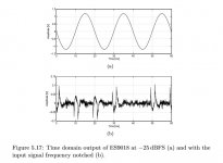
Might be worth mentioning that in addition to the FFT measurement-based hump removal info at ASR, there is a time domain measurement technique that was shared by Scott Wurcer (see attachment below).
NOTE: I tend to get attacked for saying things such as that which follows below. Apparently one can get away attacking the person not the idea by describing an idea using such terms as 'fetish.' We can at least hope that justice eventually catches up with such tricks.
To continue on the original topic, some designers have found through proprietary research that RF noise coming out of dac chip analog outputs seems to have more adverse audible effects on a differential summing stage than it does on the preceding I/V stage. Perhaps that could be related to the fact that the I/V stage using virtual ground topology which helps minimize common mode related distortion, but only that's a hypothetical at this point. (To paraphrase Jim Wilson advice on opamps: "Always use inverting topology, except for when you can't.") For whatever the underlying cause, a fix has been found which is to use additional passive filtering between the I/V stage outputs and the differential summing stage inputs. Again, I am only aware of proprietary, meaning unpublished, work in this area.
Therefore, if I were to make a change to the recommended schematic attached to post #3003 (which is a gaussian profile), I might try something like investigating by simulation dividing up the 2.74k resistors following the I/V stage into two resistors in series with some filtering capacitance added at the junction of the series resistors. It might mess up the nice gaussian filter some depending on the pole location, but it might also help improve the sound. Have to try it and see, would be my philosophical point of view.
Also, some people have suggested moving the differential summing stage farther away from the I/V stage. Its only the I/V stage that needs to be be physically close to the dac chip (although I would say maybe not too close).
Might be worth mentioning that in addition to the FFT measurement-based hump removal info at ASR, there is a time domain measurement technique that was shared by Scott Wurcer (see attachment below).
Attachments
Last edited:
To follow up on the issue of component selection for the output stage, IIRC there is a recommended BOM that can be found with the schematic at post #3003. Caps in the audio path are recommended to be NPO/C0G types. Resistors are recommended to be those with good linearity, and with close tolerances (hopefully at least .1%, maybe ideally .01%, or whatever is the lowest available tolerance is for the resistance value needed). Resistor tolerances for I/V and differential summing stages affect the ability of the output stage to suppress unwanted common mode junk from the dac outputs. As an alternate to NPO/C0G caps, some people prefer to use good quality film caps. Rolled foil and polypropylene film types are preferred by some over metalized film types. Wima is one maker of a variety of such caps.
Last edited:
Mark are you trying to found out how to solve the hump like topping did with their D50s DAC.?
But also interesting you will improve your circuit in post 3003.
But also interesting you will improve your circuit in post 3003.
Is it correct that the output section that is supplied on the recommended ES9038Q2M board has a supply derived offset that is added to one of the two outputs from the ES9038Q2M? Perhaps Vcc/2?
What is the purpose of this? Is this to aid (enable) single supply operation (along with jumper J6)? (And along with the two output blocking capacitors?)
See the attached highlighting in the enclosed picture.
Since I am not using a single supply can I remove this "feature" and the added supply noise by lifting the 8.2k resistors? [Edit: This is likely the wrong way.] The color of the ceramic dielectric of the bypass capacitors connected to those 3.3k and 8.2k resistors is obviously not NP0 or C0G. (And must be relatively small values.)
Or is that the wrong way to remove this feature? Does anyone have a schematic of the supplied output section? I guess I should start sketching it out. Perhaps I need to remove the 3.3k resistors and connect the other side of the 8.2k to ground? (As opposed to the supply derived offset voltage?)
Attachments
Last edited:
AVCC/2 is the reference voltage for the I/V noninverting opamp inputs (AVCC_L for the left channel, similar for the right channel). That's because AVCC is used to supply power to the internal dac output array resistors. Their average output voltage (if measured in voltage mode operation) is equal to AVCC/2.
It is possible to use some voltage other than AVCC/2, such as to change I/V opamp output offset voltage (e.g. set it to zero volts of offset), but that makes the current in the dac output resistor array current flow asymmetrically, say, for example, with respect to the positive and negative peaks of a sine wave. Better option is probably to remove the DC offset by some other means, such as in the differential summing stage.
It is possible to use some voltage other than AVCC/2, such as to change I/V opamp output offset voltage (e.g. set it to zero volts of offset), but that makes the current in the dac output resistor array current flow asymmetrically, say, for example, with respect to the positive and negative peaks of a sine wave. Better option is probably to remove the DC offset by some other means, such as in the differential summing stage.
Mark are you trying to found out how to solve the hump like topping did with their D50s DAC.?
Not at this point. I'm still working on my AK4499 dac. If I ever go back to ESS chips, then we'll see. Doesn't mean someone else can't do it in the meantime.
Yes, that makes sense.
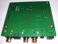
But the problem is on the supplied board I don't see a direct connection in the output section to AVCC. I have looked at the front and the back of the board and as far as I know this is a two layer board. See attached picture. No jumpers on the back from the output section to AVCC.
Instead I see the 3.3k resistors in the output section connecting to the Vcc and the ceramic bypass capacitors.
Does that mean offset from AVCC is being cancelled with a different offset derived from a different supply (+15V)? (Derived from a different supply, 3.3k Ohm resistors and small ceramic bypasses.)
Cancelling an offset from one noisy supply with a different offset generated from a different noisy supply??? What am I missing?
Attachments
There is a suggested AVCC schematic also attached to post #3003. It shows outputs that go to the I/V opamp noninverting inputs.
The stock dac board does not produce AVCC/2 signals because they are not needed by its voltage mode output stage and the DC removal caps that follow.
The stock dac board does not produce AVCC/2 signals because they are not needed by its voltage mode output stage and the DC removal caps that follow.
Yes, thank you. I understand that (post 3003) and I do plan to look into implementing the improvements. (However in a slower/more orderly fashion later on.)
But I would still like to understand what the purpose is of those 3.3k resistors and ceramic capacitors around the Pin 4/5 end of the op amp on the stock board.
Because I wonder what consequences that has to the performance of connecting those to the relatively noisy 15V supply and then the outputs of the DAC/inputs of the output stage/op amp. The only time I have seen something like that before is with single supply op amp circuits.
I am not sure this is a great idea for a high performance DAC like ES9038Q2M.
Attachments

What about audio reproduction? Which is what this forum is about.
Certainly. From the evidence of the amount of engineering efforts, hardware, expenditure and continued innovation I would suggest that audio reproduction is quite non-trivial. The book does not appear to be closed on the matter at all.
kozard,
The dac board has a solder jumper to run it from a single, say, +15v power supply. IIRC the jumper grounds the -15v rail. In that case, the noninverting input of the opamps has to be lifted above ground. It gets set to Vcc/2 IIRC. The ceramic caps are to keep the ground intact for AC purposes. If you follow the traces around its possible to sketch out the circuit. That said, one of the traces runs under the opamp socket and under one of the big filter caps, again IIRC. An ohm-meter may be helpful to trace that one.
The dac board has a solder jumper to run it from a single, say, +15v power supply. IIRC the jumper grounds the -15v rail. In that case, the noninverting input of the opamps has to be lifted above ground. It gets set to Vcc/2 IIRC. The ceramic caps are to keep the ground intact for AC purposes. If you follow the traces around its possible to sketch out the circuit. That said, one of the traces runs under the opamp socket and under one of the big filter caps, again IIRC. An ohm-meter may be helpful to trace that one.
Last edited:
Markw4; said:kozard,
The dac board has a solder jumper to run it from a single, say, +15v power supply. IIRC the jumper grounds the -15v rail. In that case, the noninverting input of the opamps has to be lifted above ground. It gets set to Vcc/2 IIRC. The ceramic caps are to keep the ground intact for AC purposes. If you follow the traces around its possible to sketch out the circuit. That said, one of the traces runs under the opamp socket and under one of the big filter caps, again IIRC. An ohm-meter may be helpful to trace that one.
Great, thank you. That is what I was trying to get at/propose/verify with post #6564.
I am going to remove that so that both the DAC and DACB connections/components to the inverting and non-inverting inputs of the op-amps both use the real ground as the reference as opposed to one (such as DACRB for example) using ground (one side of one of the 3.3k resistors) and the other (such as DACR for example) using this Vcc/2 resistor divider virtual ground.
I don't know how much of a concern it is but with different references and one being derived from the +15V supply (which supplies the 7805 and AMS1117-3.3 and everything on the board) I suspect this puts noise on the DACR side (and DACL side) that is not present on the "B" sides and thus will not cancel. (And right at one of the inputs of the op-amp.) The concern is that noise will degrade the ES9038Q2M performance significantly from the datasheet specs.
Of course multiple clean regulators and a better output section will be better still, in the future.
In reality it actually does not produce Vcc/2. At least on my boards I probed and read about 0.32V with well trimmed +/-15V and an LM4562.
kozard; said:Is it correct that the output section that is supplied on the recommended ES9038Q2M board has a supply derived offset that is added to one of the two outputs from the ES9038Q2M? Perhaps Vcc/2?
What is the purpose of this? Is this to aid (enable) single supply operation (along with jumper J6)? (And along with the two output blocking capacitors?)
Attachments

The sound reproduction book sure isn't closed on the matter of speakers and room acoustics but it is on DACs.Certainly. From the evidence of the amount of engineering efforts, hardware, expenditure and continued innovation I would suggest that audio reproduction is quite non-trivial. The book does not appear to be closed on the matter at all.
I am probably looking at it differently from you. I am not willing to consider it closed at all until the advancements and innovations are common place and widespread. (Not limited to high end chips and high end implementations.)
To me part of the equation includes the cost and widespread adoption.
Right now the top DAC technology and quality implementation is more of a unicorn that is not found in 99% of units sold. It is telling when the AKM factory/fab fire sends shock-waves through the pro-audio equipment supply chain.
To me part of the equation includes the cost and widespread adoption.
Right now the top DAC technology and quality implementation is more of a unicorn that is not found in 99% of units sold. It is telling when the AKM factory/fab fire sends shock-waves through the pro-audio equipment supply chain.
kozard,
Vcc/2 only happens when the solder jumper is used for single supply operation. Again IIRC, there is a voltage divider that sets the DC reference voltage at half way between the + and the - opamp rails. That should approximately be ground if using +-15v supplies. When the - rail is grounded for single supply operation, then the voltage divider still works the same way but one end is at ground instead of at -15v. I would agree that grounding the reference node would be better if continuing to use the voltage mode output stage. Otherwise, if using the recommended output stage then all that stuff can be removed from the board, it isn't needed.
Vcc/2 only happens when the solder jumper is used for single supply operation. Again IIRC, there is a voltage divider that sets the DC reference voltage at half way between the + and the - opamp rails. That should approximately be ground if using +-15v supplies. When the - rail is grounded for single supply operation, then the voltage divider still works the same way but one end is at ground instead of at -15v. I would agree that grounding the reference node would be better if continuing to use the voltage mode output stage. Otherwise, if using the recommended output stage then all that stuff can be removed from the board, it isn't needed.
Last edited:
Markw4; said:kozard,
Vcc/2 only happens when the solder jumper is used for single supply operation. Again IIRC, there is a voltage divider that sets the DC reference voltage at half way between the + and the - opamp rails. That should approximately be ground if using +-15v supplies. When the - rail is grounded for single supply operation, then the voltage divider still works the same way but one end is at ground instead of at -15v.
Yes, that matches what I concluded from the board. The divider consists of two 3.3k Ohm resistors and three ceramic capacitors. (The two 3.3k Ohm resistors next to the -15V bypass capacitor for the op-amp.) However when I probe I read about 0.3V (no jumper) and well trimmed +/-15V supplies.
I guess that it is 0.3V due to current through the 8.2k Ohm resistors that connect to the 6.2k Ohm resistors which then connect to DACR and DACL.
That does not occur on the other side (DACRB & DACLB) because the connections are to the real ground, not the resistor divider virtual ground.
Attachments

Last edited:
When it comes to audible sound quality in DAC technology, it is already common place and widespread. Going further in inaudible improvement isn't a contribution to the market. It only benefits the advertising world.I am probably looking at it differently from you. I am not willing to consider it closed at all until the advancements and innovations are common place and widespread. (Not limited to high end chips and high end implementations.)
To me part of the equation includes the cost and widespread adoption.
Right now the top DAC technology and quality implementation is more of a unicorn that is not found in 99% of units sold. It is telling when the AKM factory/fab fire sends shock-waves through the pro-audio equipment supply chain.
When it comes to audible sound quality in DAC technology, it is already common place and widespread. Going further in inaudible improvement isn't a contribution to the market. It only benefits the advertising world.
If you have equipment like that, great. However my laptop, desktop, SB0490 and various DAC boards I have bought in the last couple of years are not like that.
Isn't it common place and widespread that people are finding audible improvements when they go from their built-in (laptop, desktop, phone) DAC to external? I don't think all the sales of DACs and upgraded sound cards are due to advertising.
Even my FIIO X3 sounds good with headphones but something is audibly wrong when the digital out is used with a receiver with otherwise excellent D/A performance.
I don't see common place and widespread inaudible improvements. I see a lot of audibly mediocre performance in mass market products.
Basically, people are being insulted because they understand that not everything about how an audio device sounds can be predicted by commonly available measurements. For one thing, no physical device is perfectly linear and perfectly stationary. They are often close enough that we get reasonably good results by assuming weak nonlinearity and weak nonstationarity. To the extent they those things are 'weak' enough, then models assuming mathematical perfection can get us close enough for most practical purposes. IMHO not necessarily close enough for all of audio work though. Understood that some people may choose to disagree. That doesn't mean to me that it should be deemed okay to violate the rules by constant disrespectful behavior at every opportunity in which someone thinks they can get away with it.
Perhaps the human sense and capability around audio is amazing and makes the subject difficult. The ability to hear (and create, meaning musicians) is far reaching.
Whether it be human vision or human hearing we see a seemingly endless parade of increasing screen resolution, contrast, color gamut, sample rate, SNR, DNR, etc. Yet despite the quoted numbers and their hype another year passes and someone manages to do better and demonstrate it to the world.
At least it is not 1982 anymore and at least people do not say CD audio is perfect. And hopefully people have stopped saying 640k is enough. And the Olympics are no longer broadcast in NTSC format.
Nobody is insulted, it's only in your imagination. Challenging ones opinions and statements doesn't qualify as an insult whatever way you are looking at it.
The rest is the usual high end audio malarkey, "weak nonstationarity", etc... While some are using this pseudo-scientific language intended to impress the n00bs, engineers are watching the gravitational waves through a 430dB closed loop gain parametric amplifier (that's what LIGO ultimately is) and listen to signals coming from deep space with a power of -230dBW. All tools used in the process are designed using the good old engineering principles and measurements and without listening to the results.
Somehow, a group of high end audio "experts" maintain that these principles do not apply to audio reproduction and subjective, uncontrolled listening is the ultimate tool and metric. And when challenged, they feel insulted 😀.
I was insulted by you, syn08, and that was simply because I challenged you technically and found you wanting. You know nothing of my experience, knowledge or capabilities and were unable to acknowledge that you were completely wrong in one of your earlier sweeping statements. Your credibility is diminishing in my eyes with every word you type. To me your opinion or knowledge is being rendered worthless. It is a shame because you probably have very valuable experience and understanding. I'd like to think it is just your poor and childish social skills but suspect something darker drives your need to hurt and insult others. How about trying some humility? You don't know everything. An apology for insulting others here would not go amiss. Communication is about how a message is received and if someone feels insulted then to them that was the senders intention. If that was not the senders intention then their communication was poor.
I'm certain your intention is to hurt everyone here that you disagree with. I'm correct am I not?
John
I'm certain your intention is to hurt everyone here that you disagree with. I'm correct am I not?
John
- Home
- Source & Line
- Digital Line Level
- ES9038Q2M Board