At last somebody that proves me right 😉
Some points as it seems you missed some info:
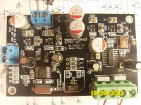
- C32 should be the other way around because an error was made. Please do this before using the DAC. It will sound better and the cap will last longer. So the - should be orientated where the + is printed on the PCB.
- Output caps of the regs should be tantalum 4.7 µF (C19, C22, C26 and C29) as the regs don't like too low ESR of ceramic caps
- a tantalum 4.7 µF tantalum for C8 is a bit better.
BTW nice build ! Nice soldering skills and, if I am not mistaking, even with lead free solder. Correct the stuff and you'll have the best DAC around Lake Ohrid !
Some points as it seems you missed some info:
- C32 should be the other way around because an error was made. Please do this before using the DAC. It will sound better and the cap will last longer. So the - should be orientated where the + is printed on the PCB.
- Output caps of the regs should be tantalum 4.7 µF (C19, C22, C26 and C29) as the regs don't like too low ESR of ceramic caps
- a tantalum 4.7 µF tantalum for C8 is a bit better.
BTW nice build ! Nice soldering skills and, if I am not mistaking, even with lead free solder. Correct the stuff and you'll have the best DAC around Lake Ohrid !
Last edited:
Thanks guys for good words about my build with special thanks to J-P for his suggestions and assistance.
I checked previous posts and it's true i missed the post with J-P explanation about C32, i'll fix this tomorow.
About tantalum, i like to build one board with ceramic and one with tanatalum caps and hear the diference.
Solder is multicore 0.5mm 60/40
I checked previous posts and it's true i missed the post with J-P explanation about C32, i'll fix this tomorow.
About tantalum, i like to build one board with ceramic and one with tanatalum caps and hear the diference.
Solder is multicore 0.5mm 60/40
Nice build Tome.
I have a question about balanced version:
The schematic shows the data signal going through R9 and R10 on the second board.
Should R9 be populated or not on the second board?
I have a question about balanced version:
The schematic shows the data signal going through R9 and R10 on the second board.
Should R9 be populated or not on the second board?
Did you mean C9 instead of C8?Yep,
Very good eye, that was an old photo, I have changed the polarity already but I have also been testing with a solen MKP in C8(1.5uf) and C32(22uf).
I cleaned the flux from pcb but still silence. I posted the voltage ratings earlier in this thread. Does anybody have any ideas?
Hi skouliki
There are some missing data's in your Post#540, DAC has 28 pins...
I'll try to give you more informations tomorrow afternoon.
Phil
There are some missing data's in your Post#540, DAC has 28 pins...
I'll try to give you more informations tomorrow afternoon.
Phil
Hi korben.
I wasnt clear- you re right. The pins i left out where connected to c10, r11, c11
DAC:
1.58--- ---0.00
1.62--- ---3.52
0.03--- ---0.00
0.00--- ---1.66
3.56--- ----0.00
1.14--- ---(-3.34)
0.00--- ---(-1.70)
0.00--- ----1.73
C10:
0.00
3.56
R11:
1.14
0.00
C11:
-1.70
1.73
I wasnt clear- you re right. The pins i left out where connected to c10, r11, c11
DAC:
1.58--- ---0.00
1.62--- ---3.52
0.03--- ---0.00
0.00--- ---1.66
3.56--- ----0.00
1.14--- ---(-3.34)
0.00--- ---(-1.70)
0.00--- ----1.73
C10:
0.00
3.56
R11:
1.14
0.00
C11:
-1.70
1.73
Hi skouliki
C10 & R11 seems fine to me, close values.
C11 is different as I've got -2.20/1.25 vs -1.70/1.73 ; 0.5V lost somewhere, check it 😉
Is it due to Pin16 = 0v ? C11 seems to be a dedicated internal ES9023 cap.
ES9023 Pins
Pin1 -> R7______________Pin16 -> ?
Pin2 -> R8______________Pin15 -> R13
Pin3 -> R9______________Pin14 -> Gnd
Pin4 -> Gnd/C10_________Pin13 -> R12
Pin5 -> C10b+___________Pin12 -> Gnd
Pin6 -> R11/C9__________Pin11 -> C12/C32-
Pin7 -> R15/C15Gnd______Pin10 -> C11
Pin8 -> R14/C14Gng______Pin09 -> C11
Pin16 is 0v on your DAC, it seems to be faulty but on the scheme there is no connexion shown... 😕
Your DAC values seems fine to me, except Pin16 and previous remark about C11.
Maybe someone more skilled than me could give an helping hand.
Last edited:
Try to power it with battery and the result is so clean and detail, dead quiet. Just one of this battery is enough for at least 6 hours of music.
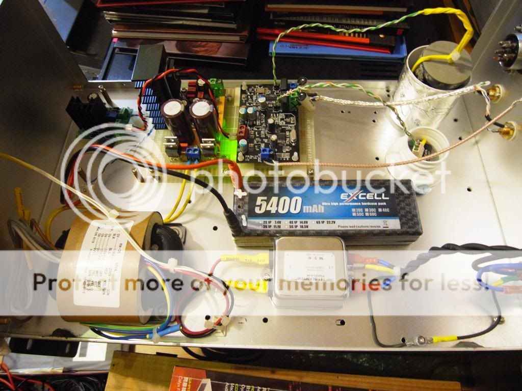
looks like a fun build, but i've gotta say, that huge film cap could not act more like an aerial if that was your goal. twisting the wires in this case does not help, if anything if it was part of a wide band amplifier it would easily cause it to oscillate. see you are twisting the same signal with an earlier version of itself, not ground or negative as is usually the case when twisting pairs.
Last edited:
no problem, have fun 😉
syklab: why have you got the case laid out like that? why not put the dac and its reception tower, erm caps ( 😉 ) all over on the right side right next to the outputs, leave all the power supply stuff over on the left side and connect DC from the regulators over the longer distances.
the dac has on-board regs anyway so if any connection can afford to be long, its those ones.
Last edited:
You know how tiring is it to keep telling to keep connections short and to clean PCB's from flux....
You know how tiring is it to keep telling to keep connections short and to clean PCB's from flux....
no, but I can imagine 😉 thats why I came back to edit and add more detail to that post, to save you from having to.
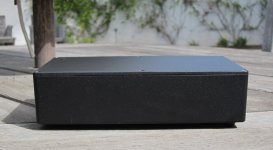
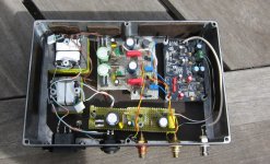
pictures of my build
I've now gotten my DAC + JG style buffer cased up and more or less completed. I housed it in a Hammond cast aluminum box, approximately 220mm x 145mm x 50mm. I managed to scrounge up some 1uf 50v BG NX and 100uf 6.3 BG N caps, so I included those in the build. The sound continues to impress me - kudos to JP and Subu. I like the sound slightly better with the JG buffer but there is a lot more cost and work associated with building it this way. One needs an extra transformer and power supply and nearly twice as much room. But the resulting DAC still is reasonably compact and I think it's worth the effort.
---Gary
Attachments
- Status
- Not open for further replies.
- Home
- Group Buys
- ES9023 / WM8804 S/PDIF DAC Group Buy