The data sheet only concerns a limit on the negative side as noone could imagen that someone would expose full B+ on the grid.I believe it’s not the max -Ve voltage you’re worried over, but a large +Ve voltage applied to the grid when the supply rail comes alive. I’ve never seen a +Ve limit quoted as a datasheet spec., but some do give a max grid dissipation limit.
Lazy designers, you don’t think that’s me? 🙂
I think lazy design also includes not understanding your circuit to decide what is needed and what is not needed.
The supersmall distance is still here and flashover will be equally easy with the grid positive as when it's negative.
By all means, skip the diode, it will work in most amps using tube rectifiers, else you will support tube industry with yet another tube purchase.
Many years ago, I built a pair of push-pull power amps that had a 6DJ8 LTP direct-coupled to a 6SN7 differential pair driver, with the cathodes of the diff pair up around 100V. I used solid-state rectifiers. The 6SN7s kept going noisy after a couple months of use, with intermittent crackling and sputtering noises getting more frequent as time went on. It's a good thing 6SN7s were cheap back then!
I didn't know what was going on then, but it's clear to me now that the grids were being pulled up to the 430V B+ with the cathodes down at ground potential ,every time I powered up the amps. Eventually I disassembled the amps. Had I know to simply put 1N4148 diodes or NE-2 neon lamps between the grids and cathodes, I might still be enjoying those amps today.
Live and learn. I'd put in the diodes and not worry any more.
Also, you'll want to add grid stoppers, especially on the cathode followers. Cathode followers run with a lot of local negative feedback, which means they tend to self-oscillate. The grid stopper will inhibit that.
These are such cheap and easy precautionary parts. Why not put them in from the get-go?
Member
Joined 2009
Paid Member
I looked at all my designs using this topology and mostly the diode is not needed so I do not needto use one in those cases, mainly it is because these designs have a safe combination of resistor values and power supply.
Additionally, cathode bypass caps and coupling caps in some cases too, all should be considered too, they must be charged up and so I mostly avoid a delayed B+ to avoid current surges through the hot tube but with a choke input power supply you may have to begin with hot tubes to prevent over-voltage of rail caps. The elegant way is understanding your circuits, then choose diodes, relays, thermistors etc. as required for the start up, shutdown and potential fault conditions.
Good reminder about grid stoppers.
Last edited:
Member
Joined 2009
Paid Member
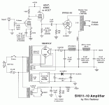
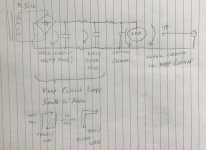
If you still have patience to spare, can you fellas review these two designs, they are both ‘on my drawing board’ for construction and both appear to contain the same topology in question although one a pre amp the other the front end of a power amp. Do you think I am safe in not using a diode in the manner we discussed above ?
I am not the original designer of course, but I believe both have been built by others, one being a commercial product. I am planning to duplicate the pre amp more or less as-is, but the power amp I will use different tubes as per my parts bin and I’ll be doubling-up to make it push-pull but it’s the same topology for the driver tubes and the tubes I’m using serve the same roles. Let’s take ‘worse case’ of SS rectifiers in both cases.
Hopefully this is considered halfways on topic!
Attachments
Last edited:
I would use them regardless, but I'd say there's a higher chance or arcing on a high mu tube than a low mu tube.
For 1.6 cents a piece, is it really worth risking the cost of a tube?
MDD(Microdiode Electronics)|MDD(Microdiode Electronics) C19357|Diodes - General Purpose|LCSC
For 1.6 cents a piece, is it really worth risking the cost of a tube?
MDD(Microdiode Electronics)|MDD(Microdiode Electronics) C19357|Diodes - General Purpose|LCSC
Member
Joined 2009
Paid Member
I just recalled that there was supposed to be a power supply, relay-timer board designed for use with the preamp board.
The seller was out and the listing on ebay was for the preamp board only.
I like this design, at least for first look it brings all the features asked, with slow start on B+, delayed mute, manual mute switch - could be useful as a pcb for other similar projects.
I like this design, at least for first look it brings all the features asked, with slow start on B+, delayed mute, manual mute switch - could be useful as a pcb for other similar projects.
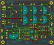
I started a first revision layout of that power supply board today,
In fact, when I looked, I had already collected 95% of the parts lol!
That's what happends when you have to many projects going at once and then from time to time life gets in the way and months go by before you look at a specific project again. I did put in an order for the parts I didn't have.
My first revision isn't all that refined as I started out with the intention on etching the board myself... I may, will most likely, refine the layout and have a boardhouse make 5 or 10 PCB's.
Keep in mind this is only a first quick and dirty layout.
As far as I could tell, the B+ part was, apart from being soft/slow started, a C-R-C....and so on design.Of course followed by the reg. circuit on the preamp PCB. The heater is merely dropped to 9V and the on the preamp board dropped to 6V. One could, if a low noise supply for the heaters is desireable use much better than 78xx regs.
Version 0.1 is because I usually do the routing at least 10 times before I feel it's good enough 😱
Attachments
Member
Joined 2009
Paid Member
I did my own etching once, single sided first and a double sided later. It's rewarding to make it all by yourself but I found it hard to justify the effort once I had discovered those low cost board houses and so now I do as you are planning, just contract it out. I find board layout a relaxing and satisfying process, I think there is some art to it and I like to end up with something that pleases my eye as well as being technically good.
You might be able to thicken up some traces for the higher current paths, mostly those carrying charging pulses to rectifiers & their first caps. There should be minimal loop area for these high pulse currents to minimize their radiating somewhere you don’t want. Grounding is also key, mainly to avoid loops and to avoid sensitive circuits sharing any ground returns with high current parts. I think you can improve on your grounding, trying for a ‘star earth’ approach might be simplest, bringing separate earth traces to a spot near the ground connector. With a two sided board you have lots of scope.
For 260V there will be some guidelines you can search up on minimum distances between adjacent conductors.
I too noticed that the main supply has a belt and braces approach. By using a long set of RC filters, a valid approach used by Shindo, Kondo etc. there should be a clean supply but there is also a zener-regulated capacitance multiplier which will itself provide a slow rise B+ without relays.
Last edited:
I did my own etching once, single sided first and a double sided later. It's rewarding to make it all by yourself but I found it hard to justify once I had discovered low cost hoard houses and so I do as you are planning, just contract it out. I find board layout a relaxing and satisfying process, I think there is sone art to it and I like to end up with something that pleases my eye.
You might be able to thicken up some traces for the higher current paths, mostly those carrying charging pulses to rectifiers & their first caps. There should be minimal loop area for these high pulse currents to minimize their radiating somewhere you don’t want. Grounding is also key, mainly to avoid loops and to avoid sensitive circuits sharing any ground returns with high current parts. I think you can improve on your grounding, trying for a ‘star earth’ approach might be simplest, bringing separate earth traces to a spot near the ground connector. With a two sided board you have lots of scope.
For 260V there will be some guidelines you can search up on minimum distances between adjacent conductors.
I too noticed that the main supply has a belt and braces approach. By using a long set of RC filters, a valid approach used by Shindo, Kondo etc. there should be a clean supply but there is also a zener-regulated capacitance multiplier.
I agree completely about the ground, as I wrote, this is just a quick and dirty layout. At first intended to be single sided, using jumper wires for the top traces.
I agree on the traces as well.
I spent maybe 2-3h on this, including the schematic. It's is very relaxing, and as you write...there's an element of personal touch/art to it as well. 🙂
The traces are just 1mm(1,5mm from the diodes to the resistors and caps), that according to google conversion is just above 39mils and just above 60mils.
If I can't get the traces to the width I'd like with a fairly compact layout, I'll add to the thickness of the Cu layers if/when ordering from a board house.
Being used to working with mostly surface mount parts, I try to make the boards as small as I can while still getting a layout that I'm satisfied with.
For me, doing layout is more relaxing than sudoku, mahjong...whatever.
I have chronic pain, and doing this takes my mind of it for a while.
6n23p
6H23∏, yes that’s the one i mean. I have a arge stash. A dozen cryoed ;^)
dave
Member
Joined 2009
Paid Member
I'm sorry to hear about your back, that really isn’t any fun. Here’s hoping your preamp finally gets finished!
Syncronicity.
A friend did up my RTP board kits, Allen was going to give me a fist gen PS he had in trad e(we had swapped Mac support for tube stuff support, and th epre-amp aains some HW i sent him) i have the big PS parts including an assembled reg. So when the case came i just put it on the top shelf and tucked the box w the boards on top.
So now, how many years later, we are doing wholesale clean-out/clean-up, we were prepping to disassemble the steel library shelf it was on. As i moved it i caught a glimpse of a tube… tha shouldn’t be there. Busy set it aside to figure out how to get into it (easy, thanx for that Scott), and low and behold. ARC SP10 clone boards with a skookum looking PS, R-Core trafo, and some sort of fancy volume control.
Further, when i was in my last year at UofA (1976) i drew up boards for the, then reining, SP3A. Made PCBs forgot to mirror the drawing before sending it away. That same friend took the boards and hacked a working preamp together. It got used a lot before it got killed as a victim of being in the trunk when i was rear ended.
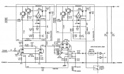
Looking at the SP10 circuit it too has a DC CC->CF in it, but not a simple one with a pararlled ECC88 (i guess to push impedance down further). The extra initial gain stage seems superfluous… the PS stuff loading the tbes might be informative.

u
dave
A friend did up my RTP board kits, Allen was going to give me a fist gen PS he had in trad e(we had swapped Mac support for tube stuff support, and th epre-amp aains some HW i sent him) i have the big PS parts including an assembled reg. So when the case came i just put it on the top shelf and tucked the box w the boards on top.
So now, how many years later, we are doing wholesale clean-out/clean-up, we were prepping to disassemble the steel library shelf it was on. As i moved it i caught a glimpse of a tube… tha shouldn’t be there. Busy set it aside to figure out how to get into it (easy, thanx for that Scott), and low and behold. ARC SP10 clone boards with a skookum looking PS, R-Core trafo, and some sort of fancy volume control.
Further, when i was in my last year at UofA (1976) i drew up boards for the, then reining, SP3A. Made PCBs forgot to mirror the drawing before sending it away. That same friend took the boards and hacked a working preamp together. It got used a lot before it got killed as a victim of being in the trunk when i was rear ended.
Looking at the SP10 circuit it too has a DC CC->CF in it, but not a simple one with a pararlled ECC88 (i guess to push impedance down further). The extra initial gain stage seems superfluous… the PS stuff loading the tbes might be informative.
u
dave
Attachments
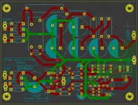
V.0.2 of ? lol
I did another quick shuffle of the parts and routing.
Now most traces are 2mm wide, that is about 78.7mil.
I know I'm not there yet, but each time I re-do a layout (the same thing with just about every project) I learn something new. That is what we're in this crazy thing called DIY in the first place, isn't it? To have fun and learn things.
Anyway here comes the second quick and dirty layout.
Attachments
Member
Joined 2009
Paid Member
What I do is to layer the earth return traces according to how ‘dirty’ the are. I like to get the dirty currents sunk first, to a star ground (which is usually located at the ‘earth’ side of the PSU capacitor and where speaker return is connected if in a power amp). Then all the dirty currents are kept to a small loop local to the power supply. I then layer-on additional earth traces for cleaner signals. Of course, it’s not a ‘follow blindly’ method, but a starting point and depending on details maybe modified.
So on your pcb I’d be using all available area to fill copper over the connections for the diodes, main caps and connections to the AC supply from the power transformer. Keeping all those areas tightly grouped etc. In my layout software you can create solid polygons to make full use of the available space.
You have gnd returns coming in like branches of a tree but they’re coming in from filter caps and sensitive circuits all along the trunk. It maybe fine but I usually don't like to do that. You could create a local star ground point for all the small signal return currents and the tie that into the main star ground with one trace. I’d also move the gnd connector closer to the diodes/fist cap to keep high current spikes contained to a small area.
Some layout techniques work better with a ground plane, but you really need to be careful about cuts and return paths.
I hope you don’t mind my nit picking!
Attachments

Last edited:
What I do is to layer the earth return traces according to how ‘dirty’ the are. I like to get the dirty currents sunk first, to a star ground (which is usually located at the ‘earth’ side of the PSU capacitor and where speaker return is connected if in a power amp). Then all the dirty currents are kept to a small loop local to the power supply. I then layer-on additional earth traces for cleaner signals. Of course, it’s not a ‘follow blindly’ method, but a starting point and depending on details maybe modified.
So on your pcb I’d be using all available area to fill copper over the connections for the diodes, main caps and connections to the AC supply from the power transformer. Keeping all those areas tightly grouped etc. In my layout software you can create solid polygons to make full use of the available space.
You have gnd returns coming in like branches of a tree but they’re coming in from filter caps and sensitive circuits all along the trunk. It maybe fine but I usually don't like to do that. You could create a local star ground point for all the small signal return currents and the tie that into the main star ground with one trace. I’d also move the gnd connector closer to the diodes/fist cap to keep high current spikes contained to a small area.
I hope you don’t mind my nit picking!
It's getting obvious I've been doing mainly digital circuits and using the small, mainly 0402, 0603, 0805 and 1206/1210 for passive components...it really does help layout. That and gnd-planes with different prioritys, kicad allows for multiple zones.
I'll keep at it. I was not really happy with this second version either...I did feel it better than the first but not by much.
TBH, I'm more comfortable with 0.5mm pitch SMD than I am with througn hole parts these days.
The first layout, not the routing just the layout, is how the parts were laid out on the PSU PCB that wasn't available when I got the ECC88 preamp PCB. I did get the schematic, BOM and a print out of the top silkscreen.
I could e-mail you the info, just not comfortable sharing to much on a forum without the creators permission. Drop me a PM if you're interested in seing how the guy that designed it had it laid out etc.
Thank you for the constructive critique, I never mind getting that....that's how we learn after all.
I decided to do one more before calling it a night.
I'm not saying it's much better, just playing around for now.
Dimensions are 150*120mm, so close to the largest board I've ever done a layout for, with the least amount of components as well lol.
The zones are clumsy and connection between them are ugly, but I wanted it done as I sorely need to rest my back (no pun intended).
Let's get some more constructive critique 🙂
Attachments
Member
Joined 2009
Paid Member
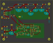
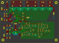
I like the changes. You might be able to move that relay so that the first cap after the diodes at the top can be placed close to the diodes like you have it on the bottom. I’d pull back the gnd plane away from that 250V connector as high voltage needs space around it. Some of those red traces at the caps could be polygons too, these connections carry as much current as the gnd connections.
I did another quick shuffle of the parts and routing.
Now most traces are 2mm wide, that is about 78.7mil.
I know I'm not there yet, but each time I re-do a layout (the same thing with just about every project) I learn something new. That is what we're in this crazy thing called DIY in the first place, isn't it? To have fun and learn things.
Anyway here comes the second quick and dirty layout.
I know the feeling.
I've been working up literally over seven different Circuits at once for PCB's each one of them presented different challenges to learn. 3 amps (Darling, Rh84 SE, Broskie el84 PP); 2 pre amps (Franks 6sn7 direct couple; Salas 6v6 in mono); 1 filament supply with capacitive multiplier; and several small CCS "shield boards". I know It sounds crazy this shotgun approach, to just grab schematic after schematic and draw pcb boards, but it did accelerate my learning this. The main thing I learned is to not send the board for mfg until Ive reworked it many times. Discovering an improvement in one board Ill go back and apply to all of them. Its an addiction now.
Last edited:
Member
Joined 2009
Paid Member
It takes me weeks until I’m happy with a layout, it’s even been known to require me to redo from scratch if the appearance troubles me. I only tape out once it feels right. I’d be hopeless as a professional because it takes me too long and I’d stop enjoying it. I have never been tempted to ruin my hobby by trying to make a living off it, assuming my stuff was even good enough for that anyhow!!
I suspect board layout for some of us is akin to calligraphy for others.
I suspect board layout for some of us is akin to calligraphy for others.
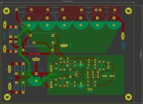
I made two versions this morning after having walked my daughter to daycare.
Lets call them option A & B, B being the one with ferrite beads separating the B+ GND from heater and timing/relay-related circuit GND.
Lets call them option A & B, B being the one with ferrite beads separating the B+ GND from heater and timing/relay-related circuit GND.
Attachments
- Home
- Amplifiers
- Tubes / Valves
- ECC88 PreAmp - Questions