I have too many projects right now but perhaps I should try to layout my own board. The package is not that hard to solder. I wonder if anyone has done a four layer DAC board at JLCPCB? (Setting up KiCad properly might be a good portion of the work.)
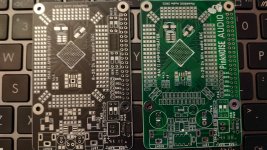
I did a 4-layer at JLCPCB. Worked okay. Solder mask wasn't as robust as a similar board from PCBWay. Pushing a solder iron tip lightly across it, wasn't too hard to scratch off a few little streaks of mask material while hand soldering some fine pitch SMD. Of course, that didn't have anything to do with it being 4-layer.
As a side note, might mention to keep costs down I limited via hole sizes to no smaller than 0.5mm. Always good to see what features a board house will charge extra for before laying out a board.
As a side note, might mention to keep costs down I limited via hole sizes to no smaller than 0.5mm. Always good to see what features a board house will charge extra for before laying out a board.
Mark, have you ordered black solder mask? It is not as robust as in green case at JLCPCB. From now, I will order only green solder mask since it is very good.
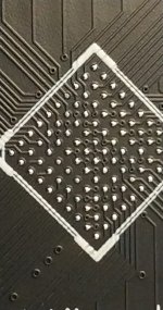
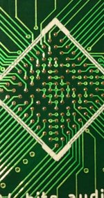
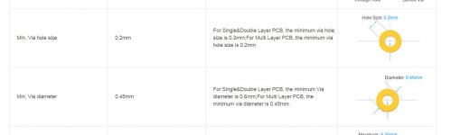
In case of 4-layers PCB, the minimum holes for vias is 0.2 mm, outer vias diameter 0.45 mm, with no any extra cost. Look at the vias under CPLD, which is FBGA package having 1mm distance between pads.
In case of 4-layers PCB, the minimum holes for vias is 0.2 mm, outer vias diameter 0.45 mm, with no any extra cost. Look at the vias under CPLD, which is FBGA package having 1mm distance between pads.
Attachments
Did either of you use KiCad for the four layer layout?
How did you utilize the layers? Top for signal? Bottom GND? The layer under the top layer for power planes?
How did you utilize the layers? Top for signal? Bottom GND? The layer under the top layer for power planes?
You mean the pictured (attached image) board is not recommended? And that one is oscillating? (Even after the X5R caps were added on the bottom side?)
Did you ever solve the oscillation problem or did you have to scrap it?
I have one of these boards laying around.
I also have my own, untested, dual PCM1794 Boards.
I recall trying two of the single PCM1794 Boards getting single ended out via transformers.
This was a long time ago and I don't remember how it worked out. It was a Ciry or something like that design.
IIRC, the circuit is more or less the datasheet application for dual PCM1794. I don't know how the board is layed out.
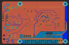
I use Eagle, but yes, I used top for signal, bottom GND, and the other layers for power planes, and I take care to insert GND in these middle planes, under the signal traces, where this is possible. Look at the picture below. You can figure out what is the GND area in this orange power plane.Did either of you use KiCad for the four layer layout?
How did you utilize the layers? Top for signal? Bottom GND? The layer under the top layer for power planes?
Attachments
Great. Thank you.
Is Eagle still free for a board like that? Or is it a paid program now? It is complicated to setup Eagle for ordering at JLCPCB? (Design rules, etc?)
Is Eagle still free for a board like that? Or is it a paid program now? It is complicated to setup Eagle for ordering at JLCPCB? (Design rules, etc?)
Mark, have you ordered black solder mask?
It was green but the cheap boards, not an upscale version. Regarding hole sizes, if you go to the quote page under advanced settings, looks like minimum is .45mm (which I may have rounded up to .5mm in my head). Smaller is optional. To quote:
"High-precision PCBs with 0.2/0.4mm Via are much more difficult to produce. To ensure the board quality, “ 4-Wire Kelvin Test” and “FR4 Tg155” options are automatically selected when 0.2/0.4mm has been chosen."
Could be there are drill charges for that too, dunno.
Last edited:
I recommend KiCad highly, I make mostly 4 layer PCB these days. Top and bottom layers typically signal and ground, inner layers power and sometimes some signals also routed.
The PCM7194 has two differential DACs incorporated, in mono mode you can wire the outputs in parallel to sum output current - but read the application notes in the specification there is a caveat. (In mono mode the phase of one channel gets reversed.)
I designed a dac using the PCM1794 in parallel mono mode about a decade or so ago, was entirely satisfactory.
How did you utilize the layers? Top for signal? Bottom GND? The layer under the top layer for power planes?
Used Circuit Studio. Top was sensitive signals and ground fill, 2nd was all ground fill and a few short signal trace duck-unders, 3rd was power rail(s) fill areas with a few short signal trace duck-unders. 4th layer was different with different versions of the board, for one board control circuitry and voltage regulators were on the bottom along with some ground fills. quite a few long control signal runs on the bottom too. Everything was laid out to minimize unwanted stray coupling. Just have to figure out what makes sense for a given project, then prototype for test to see if a revision is needed.
Last edited:
@kozard
I don't know, because I have paid version of Eagle at the company I work for.
@Mark
The values you reffer to are for vias outer diameter, not for their holes. As I told you, if you have an BGA package having 1 mm pitch or 0.8 mm (hard, but possible) is OK, but if you have one with 0.5 mm pitch balls, the PCBs are very expensive.
Attachments
I recommend KiCad highly, I make mostly 4 layer PCB these days. Top and bottom layers typically signal and ground, inner layers power and sometimes some signals also routed.
Do you use a template to start your KiCad 4 layer layouts for JLCPCB (or do you fab somewhere else?) to help make sure things are setup right? Or do you just manually setup minimum and default via, pad and trace rules yourself?
Having not used KiCad I am a little concerned about messing up the first four layer board order with silly mistake. I am searching online for a KiCad project that I can download and use as a starting point to hopefully avoid a silly (setup) mistake and wasting the boards.
The PCM7194 has two differential DACs incorporated, in mono mode you can wire the outputs in parallel to sum output current - but read the application notes in the specification there is a caveat. (In mono mode the phase of one channel gets reversed.)
I designed a dac using the PCM1794 in parallel mono mode about a decade or so ago, was entirely satisfactory.
I have a couple schematics that others have verified as working. However I would like to try making a layout carefully with four layers and some better components than I have seen on the eBay/AliExpress boards. Maybe more along the lines of DDAC. But I plan on only one pair and I will use a separate decoder board. I might do the layout in such a way that an extra board could be used for the IV section on my ES9038Q2M board that needs some help.
I quite like the PCM1791 in a used receiver I bought (and PCM1702) in another used buy. But I would like to see what I can do if I carefully do the layout and use better components, power supplies, etc. I am getting tired of the "cheap" DAC boards that always have problems.
Did either of you use KiCad for the four layer layout?
How did you utilize the layers? Top for signal? Bottom GND? The layer under the top layer for power planes?
yes, I used a 4-layer layot.
No templates are required with KiCad or JLCPCB, just make sure that you generate standard gerber files at the end of the process. (You need to select the gerber layers when you generate them.) I use JLCPCB for most things these days and haven't had an issue.
The minimums per industry norms are all default settings in the board setup file
You don't want to carry over setups from other boards, this is how mistakes are made. The default settings are fine, and you can review your gerber files in the included gerber viewer. In addition there is DRC (design rule checking) and the default settings are compatible with JLC.
KiCad is open source and free, there is lots of online support. There is a significant learning curve but I have managed good results on more than 70 PCB layouts so far.
You can import Eagle PCB files and footprints, although not using Eagle I have never tried this.
Attachments
I am making progress with the PCM1794 board and I tested the first board with a PCM1798 so I would not waste a PCM1794. (Just in case something was not fixable.)
It turns out to be working. There was one mistake on the Vcm bypass which was easily fixed and did not stop it from working.
However initially it appears to be not working since the left channel was fine (-115 2nd Harmonic) while the right channel was terrible (huge -70 dB noise floor). I probed everything, swapped op-amps and even swapped the PCM1798 but the result did not change. I switched it into mono mode and either both outputs were great (left channel select mono mode) or both channels were terrible (right channel select mono mode). It turned out that hanging a second WM8805 (transmitter) off of the WM8805 receiver (connected to the DAC) somehow messed up the signals.
I had the second WM8805 there so that I could see the input to the PCM1798 via a digital loop-back. I thought testing the digital loop-back (to ensure I had a good signal and right format at the PCM1798) would prevent a problem. Instead it seems to have degraded the signals. [Yet the WM8805 to WM8805 SPDIF loopback was perfect.]
I removed the second WM8805 (monitoring transmitter) and suddenly everything was ok in both stereo and mono mode. Unfortunately I do not have a high speed scope so I can't say what exactly happened (reflections/ringing/etc).
So I have a question. My intention is to assemble two boards and run them in mono mode. The single board worked fine in mono mode today.
But if I have trouble just connecting a second WM8805 I was wondering what the best practices are for connecting two PCM1794 to one WM8805 without messing up the signal? What are the best practices such as layout, resistors (ringing?), etc? I hope I don't need to use buffers (I doubt that is needed).
Last edited:
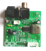
The WM8805 is not on my own board. My own board just has the PCM1794/8, I/V stage and several very low noise regulators.
I have bought WM8805 chips but I have not done that board yet. I just bought a simple WM8805 board to debug my DAC design. (Picture attached.) Later I plan to design a better board or buy and use a better SPDIF to I2S receiver. Right now I have not dug into WM8805 datasheets or the design of the board I am using. It was intended as something temporary to test my design for signs of life. So far with even the PCM1798 test chip installed the performance exceeds my E-MU 1616m ADC which is the best I have. When I get further along I will test with OAP1612 and with the hall notch filter.
Basically I am making my own PCM1794 board and then comparing it with my LJM CS4398 and the modified ES9038Q2M. When I decide which is the best of the best I will make a second spin for the one that I like best. I am also comparing it with the CS4398 inside the E-MU 1616m which has had some upgrades and is awaiting op-amp upgrades. The 1616m has (as far as I can tell) very low noise supplies and low jitter clocks (at least claimed and well regarded). I like my modified ES9038Q2M but I do like the BB parts in my Denon receivers so I thought I would compare the different designs leisurely over the next year or so. I have upgraded various bits inside the Denons and they are also slated for op-amp upgrades next for the BB PCM DACs.
Recently I obtained real OPA1612 and OPA2134 to add to the mix also. (Previously my best were LM4562NA and then the old NE5532.)
Attachments
I ran two PCM1794A in mono mode and had a lot of problems until I added 22R (IIRC) series termination resistors at the WM8805 I/O.
- Home
- Source & Line
- Digital Line Level
- Ebay parallel PCM1794 DAC any good