i found this board. it looks with less components for the LM1875
SUQIYA 20W Gaincard version of the two channel LM1875 power amplifier kit finished board tube flavor-in Amplifier from Consumer Electronics on AliExpress
SUQIYA 20W Gaincard version of the two channel LM1875 power amplifier kit finished board tube flavor-in Amplifier from Consumer Electronics on AliExpress
yes i remember/ and note it😉
composite amplifiers
is the DC/compisite better soundwise? or what advantages?
chris
With a composite amplifier coupling, you let an OP-AMP control a power amplifier chip such that it is the OP-AMP that dominates the sound quality. The OP-AMP controls the power amplifier chip as a "slave" and uses the power amplifier chip for its output stage.
As OP-AMPs often have much less THD than power amplifier chips, you can achieve very low THD values with the composite amplifier coupling. This is what Neurochrome/Tom uses. Further, it will be the input offset of the OP-AMP that decides the output offset such that also the output offset becomes less.
In principle you can use any power amplifier chip with sufficient power capacity but it is advised to use a power amplifier chip with low THD and good stability margin.
I found the component values that Brian Bell used for the Chipamp.com LM1875. There is an option for the minimum configuration so will give that a try. I have a couple of chips and a heatsink so have ordered 2 more PCBs.
When done I'll post it.
When done I'll post it.
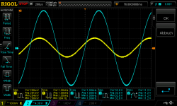
amp2_ripple idle/ load 8R
Hi
the amp 2
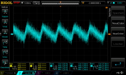
amp2 has the recovered lm1875 and the 4,7µF wima as input cap+ a 22µF ues green nichicon feedback cap. 1000µF/50 supply caps per rail at the pcb + bigger psu cap bank about 15000µF per rail measured.
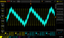
pic 1 +2 are the idle ripple at V-, V+ at the cap bank board without load
pic 3+4 100mmVrms at 8R/0,7W ripple at V-, V+ at the cap bank board
pic 5+6 200mmVrms at 8R/2,6W ripple at V-, V+ at the cap bank board
pic 7+8 400mmVrms at 8R/10,7W ripple at V-, V+ at the cap bank board
chris
BTW: if you see at the input scope - yellow sometimes different values at the same measurements - i found that my probe is defective :-(
Hi
the amp 2
amp2 has the recovered lm1875 and the 4,7µF wima as input cap+ a 22µF ues green nichicon feedback cap. 1000µF/50 supply caps per rail at the pcb + bigger psu cap bank about 15000µF per rail measured.
pic 1 +2 are the idle ripple at V-, V+ at the cap bank board without load
pic 3+4 100mmVrms at 8R/0,7W ripple at V-, V+ at the cap bank board
pic 5+6 200mmVrms at 8R/2,6W ripple at V-, V+ at the cap bank board
pic 7+8 400mmVrms at 8R/10,7W ripple at V-, V+ at the cap bank board
chris
BTW: if you see at the input scope - yellow sometimes different values at the same measurements - i found that my probe is defective :-(
Attachments
-
 idle ripple at 8R at V- Rchannel.png78.5 KB · Views: 225
 -
 400mVrms input V+ with 8R Rchannel_10,7Watt.png88.5 KB · Views: 97
 -
 400mVrms input V- with 8R Rchannel_10,7Watt.png87.6 KB · Views: 86
 -
 200mVrms input V+with 8R Rchannel_2,6Watt.png86.4 KB · Views: 81
 -
 200mVrms input V- with 8R Rchannel_2,6Watt.png83.1 KB · Views: 223
 -
 100mVrms input V+ with 8R Rchannel_0,7Watt.png93.4 KB · Views: 238
 -
 100mVrms input V- with 8R Rchannel_0,7Watt.png93.8 KB · Views: 235
 -
 idle ripple at 8R at V+ Rchannel.png71 KB · Views: 237
Last edited:
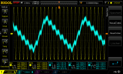
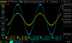
amp ripple at 4R
Hi
the same amp with 4R- this recovered chip shows again its ocp!
pic 1 100mmVrms at 4R/1,34W ripple at V- at the cap bank board
pic 2+3 200mmVrms at 4R/5,1W ripple at V-, V+ at the cap bank board- strange jumping
here is the output at 200mVrms input- every second switch off
at 4,52V rms-13Vpp - it is just 1,13A into 4R so it should not go into ocp!!
neertheless i will try to mod the recovered chipt as FF wrote in the previous post :
A genuine chip I find is a good idea. My suggestion serves for you (and us) to learn more about the tricks that are available when we end up in trouble, and that may only be with a "fake" chip.
chris
Attachments

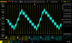
...recovered chip healed...
Hi
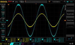
thanks to FF !
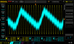
at post 320 i see at the recovered chip this ringing at the top of the positive sine wave. in post i get the hint by FF (post 334) to use a resistor between pin 1 + 2 and start with 1k.
finally i got:
with 1k (994,3R) i got a DC offset Voltage of -83,5mV - that is to much ---> i use 2k7 (2687R) and get 34,3mV DC offset and no ringing at 500mV
should i try to get less DC offset?
pic 1 is with 400mVrms input and no ringing at 8R - its about 10,2Watt each channel
pic 2 is with 500mVrms input and no ringing at 8R - its about 15,7WAtt
with 600mVrms in i get ringing at the top but not really as much as in post 320
chris
Hi
thanks to FF !
at post 320 i see at the recovered chip this ringing at the top of the positive sine wave. in post i get the hint by FF (post 334) to use a resistor between pin 1 + 2 and start with 1k.
finally i got:
with 1k (994,3R) i got a DC offset Voltage of -83,5mV - that is to much ---> i use 2k7 (2687R) and get 34,3mV DC offset and no ringing at 500mV
should i try to get less DC offset?
pic 1 is with 400mVrms input and no ringing at 8R - its about 10,2Watt each channel
pic 2 is with 500mVrms input and no ringing at 8R - its about 15,7WAtt
with 600mVrms in i get ringing at the top but not really as much as in post 320
chris
Attachments

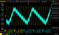
Hi
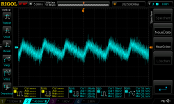
the ringing starts at 500mVrms input (15,7W at 8R)
pic 1 with 2k7 resistor at the R channel (DC offset 34mV)
pic 2 original at the L channel (Dc offset -1,5mV)
- more power get worse at both versions..not really a difference
520mVrms input - 16,8Watt at 8R
pic 3 with 2k7 resistor at the R channel (DC offset 34mV)
pic 4 original at the L channel (Dc offset -1,5mV)
chris
Attachments


Chris, i read your contributions with much interest and i will soon try to replicate your experiments and findings (?).
As far as the ringing artifacts are concerned i remember to have seen a very interesting explanation on the use of ferrites to avoid parasitic oscillation, especially look at a convincing issue at about 9:51 of the flw youtube presentation - see here YouTube
So maybe you could try to insert a ferrite bead over point 1 and/or 2 of the LM1875t. Obviously this should not have an effect on the audio signals.
In the meantime i received my (audio) SMPS + and -24V at 6 A and i quickly had a quick first look at my Rigol scope. The unit really looks elegant, small and well engineered. I could adjust the output voltage between approx plus and minus 23 and 29V.
At 29V ( 58v) the genuine LM1875t should deliver about 40W of clean power according to the interesting test of JohnAudioTech Youtube session, so that looks very interesting (more than enough for me).
However when testing the Powersupply i noticed that testing a SMPS unit is not simple. The 29V output on the scope (with a 16 ohm load) shows about 100mV ripple, but frankly the waveform is of a rather nasty and complicated switching/oscillatory nature. When moving the scope probe near the transformer, it picks up relatively strong hf oscillations in the range 150 up tp 500Khz. So i will first build the powersupply in a screened and closed aluminium box, with an additional input rf filter and see the results
Not sure whether that small HF ripple will have an adverse inpact on the noise / audio performance, but first i will take the time to further investigate and hopefully cleanup the output of the powersupply
Hi
the ringing starts at 500mVrms input (15,7W at 8R)
pic 1 with 2k7 resistor at the R channel (DC offset 34mV)
pic 2 original at the L channel (Dc offset -1,5mV)
- more power get worse at both versions..not really a difference
520mVrms input - 16,8Watt at 8R
pic 3 with 2k7 resistor at the R channel (DC offset 34mV)
pic 4 original at the L channel (Dc offset -1,5mV)
chris
Once more very good work, Chris.
You can for learning eventually try to raise the resistor value to 4K7 to see if that is still good enough. The lower the resistor value, the lower the effective feedback correction and thus higher THD and higher output offset. Nothing is for free. The resistor value needed may be individual for each 'fake' LM1875 specimen.
The most important for you is to have a further tool in your toolbox for when you run into such stability issues. The self-oscillation seen is perhaps a difference in stability between a 'fake' and a genuine.
If you really wanted to make a good amplifier with the 'fake' LM1875, perhaps the 1K resistor could be used and a controlling OP-AMP (composite amplifier configuration or even DC servo configuration) used to reduce the output offset (and THD if used in the composite configuration). You should try such a 'controlling OP-AMP' at a certain moment. For now, you may also continue with the genuine LM1875s instead of working on compensation of weak specimens. Then, you can spend more time on listening and draw conclusions between class AB and class D sound.
Since three very active years for you with DIY electronics, you can now realize how much you have learned about controlling and improving amplifier circuits. Today you learned one more trick. There are a few more tricks to learn but you progress very fast. With good knowledge, you can decide when to take a construction towards perfection or to stop a project when almost all learning has been gained. After all, we need only one amplifier at a time and having the basement full of optimized amplifiers is as such a waste (apart from the knowledge that was gained).
Last edited:
Hi FF
Thanks but it is your work too - because you help a lot of noobs like me.
Thank you FF
🙂
LM1875 journey is not finished for me.
1 next Step - LM1875 kit with genuine parts -still ordered and on my bench 😀
2 composite amp --> power is nothing without control 😛
chris
Thanks but it is your work too - because you help a lot of noobs like me.
Thank you FF
🙂
LM1875 journey is not finished for me.
1 next Step - LM1875 kit with genuine parts -still ordered and on my bench 😀
2 composite amp --> power is nothing without control 😛
chris
5k at the inputs to avoid ringing
Hi
i did tthe "healing" at the other channel with 10k//10k so i get about 5k and -17mV DC at the output. load is 8R at both channels.
better at 500mV but at higher power the same.
pic 1 +2 with 5k, without (original)
pic 3+4 550mVinput with 5k, without
chris
Hi
i did tthe "healing" at the other channel with 10k//10k so i get about 5k and -17mV DC at the output. load is 8R at both channels.
better at 500mV but at higher power the same.
pic 1 +2 with 5k, without (original)
pic 3+4 550mVinput with 5k, without
chris
Attachments


I believe the LM1875T delivered with the kit could very well be this Unison LM1875T.
For the datasheet look here
That does not look bad
Fred
I believe you could be right. Pretty similar to TI specs.
As I recall it, the LM1875 design dates back to around 1990. It is more than unlikely that Asia, in 2019, cannot come up with similar specs as "the West" 30 years before.
Asian chip designs are generally up to specs and on par with most of what we find among brands we know.
There seems to be a tendency of "die-schrinking", which is logical from an economical point of view but may mean that such die-schrinked items are closer to the spec. limits than we are used to.
I find it unlikely that someone in Asia let incompetent chip designers make an own new (poorly performing) wafer design for large-scale production, marked as TI chips, to be sold at very low prices. More likely, what we find at very low prices are those items that did not pass the production tests for one reason or another, remarked items of a known but less performing type (TDA2030 -> TDA2050) or die-schrinked versions of existing genuine designs.
Last edited:
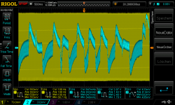
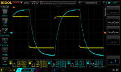
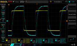
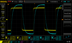
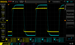
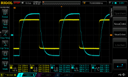
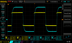
square wave stability...
Good Evening
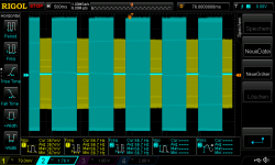
i did at my recovered chips the modifications with the 2k7 (Rchannel)or 5k (L channel)at pin 1-2. for this configuration i look at the square wave stability with 8R load and a 440nF mkt cap at the spekaers terminal.
the 100pF is in parallel with the feedback 22k resistor. at this chip i got the ocp at 400mVrms input (as always) into 8R. (about 10W) -- both channels are identical
i checked it.
pics
100mVrms in 10k, 20k, 30k
200mVrms in 10k, 20k, 30k
400mVrms in 10k, 20k, 30k - ocp hick in - i set the scope to single
so everything fine.
chris
but look at the next post
Good Evening
i did at my recovered chips the modifications with the 2k7 (Rchannel)or 5k (L channel)at pin 1-2. for this configuration i look at the square wave stability with 8R load and a 440nF mkt cap at the spekaers terminal.
the 100pF is in parallel with the feedback 22k resistor. at this chip i got the ocp at 400mVrms input (as always) into 8R. (about 10W) -- both channels are identical
i checked it.
pics
100mVrms in 10k, 20k, 30k
200mVrms in 10k, 20k, 30k
400mVrms in 10k, 20k, 30k - ocp hick in - i set the scope to single
so everything fine.
chris
but look at the next post
Attachments
-
 square 400mVrms 30khz in 8R with 440nF L channel _5k pin 12_ocp.png47.5 KB · Views: 97
 -
 square 400mVrms 20khz in 8R with 440nF L channel _5k pin 12_ocp.png50 KB · Views: 85
 -
 square 400mVrms 10khz in 8R with 440nF R channel _2k7 pin 12_ocp.png45.9 KB · Views: 84
 -
 square 200mVrms 30khz in 8R with 440nF L channel _5k pin 12.png47.4 KB · Views: 88
 -
 square 200mVrms 20khz in 8R with 440nF R channel _2k7 pin 12.png51.2 KB · Views: 81
 -
 square 200mVrms 10khz in 8R with 440nF R channel _2k7 pin 12.png51.2 KB · Views: 88
 -
 square 100mVrms 30khz in 8R with 440nF L channel _5k pin 12.png46.9 KB · Views: 92
 -
 square 100mVrms 20khz in 8R with 440nF R channel _2k7 pin 12.png50.2 KB · Views: 81
 -
 square 100mVrms 10khz in 8R with 440nF L channel _5k pin 12.png49.3 KB · Views: 223
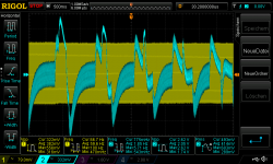
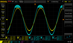
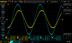
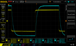
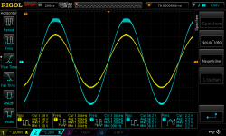
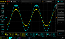
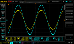
What i do not expect is that if i switch from square to sine wave i normally get a destroyed ringing at the top of the upper sine wave above 400-500mVrms - this is why i get the hint to use the reeistor between pin 1 -2 (2k7 or 5k)
look at post #347 or #320
now with 440nF at the output it gone.
examples:
pic 1 shows 550mVrms with 440nF at the output
pic 2 the same power without the 440nF at the output
pic 3 shows 600mVrms with 440nF at the output
pic 4 the same power without the 440nF at the output
pic 5at my input 620mVrms
??? why does the 440nF healed here???
chris
Attachments
-
 550mVrms sine wave with 440nF at the L-Channel 5k pin12.png49.6 KB · Views: 97
 -
 550mVrms sine wave without 440nF at the L-Channel 5k pin12.png50 KB · Views: 94
 -
 600mVrms sine wave with 440nF at the R-Channel 2k7 pin12.png50.7 KB · Views: 96
 -
 600mVrms sine wave without 440nF at the R-Channel 2k7 pin12.png51.3 KB · Views: 98
 -
 620mVrms sine wave with 440nF at the L-Channel 5k pin12_24Watt.png51.5 KB · Views: 96
This seems like an OK place to ask this question:
I had some boards made based on BrianGT's LM1875 boards and the datasheet schematic (very similar either way). I'm using a PS-SS from Glass-ware and a 30VA CT transformer. I was measuring about 22-23V on either side of the power supply before hooking it up to the board. When I hooked it up to the board, the chip popped!
I've made many LM1875 amps using protoboard, point-to-point, other PCBs, and many different power supplies, as well as what were likely fake chips and real chips. All of them so far have functioned without issue. These chips I ordered from Mouser and should be real. This is the first time a chip has popped. It happened almost instantly after applying power. What do you think could have caused this? There was no input or output hooked up, only power. It was mounted on a hefty heatsink.
This seems like an OK place to ask this question:
I had some boards made based on BrianGT's LM1875 boards and the datasheet schematic (very similar either way). I'm using a PS-SS from Glass-ware and a 30VA CT transformer. I was measuring about 22-23V on either side of the power supply before hooking it up to the board. When I hooked it up to the board, the chip popped!
I've made many LM1875 amps using protoboard, point-to-point, other PCBs, and many different power supplies, as well as what were likely fake chips and real chips. All of them so far have functioned without issue. These chips I ordered from Mouser and should be real. This is the first time a chip has popped. It happened almost instantly after applying power. What do you think could have caused this? There was no input or output hooked up, only power. It was mounted on a hefty heatsink.
I understand your surprise. Did you notice if the chips got very hot when you connected the power? If the chips for some reason started self-oscillation they heat up very fast. Did you short the inputs before you put power on? Leaving the inputs open is an invitation to oscillation.
- Home
- Amplifiers
- Chip Amps
- eBay mono LM1875 kit