Well, for now it works. If later i see that it does not work properly i will somehow try to use a dedicated IC for synchronous buck converters but it needs to be capable of sensing up to 40A and a voltage that goes up to 80 - 90V. The IC will be powered with just 12 - 15V f course. There is a small buck converter that powers the driving stuff (it can take 120V maximum at its input). So up to 100V input voltage should be safe.
Once, i actually tried to design an ISOLATED half bridge converter. But i'm not very good at winding transformers. Its quite hard and requires a lot of patience... And copper. Expecially for 40+ Amps.
Like this, i could have made a single supply to dual supply converter. But i failed. Since the output of those converters is completely isolated, they could be connected in series and that makes the dual supply possible.
This stuff is very hard to do, winding good transformers by hands is not easy. For such a thing i would literally need an actual electronic engineer helping me in real life.
Such projects do also take a lot of time, which i dont always have.
I even managed to find 'empty' transformers online that i can wind myself.
For converters in general, i'm planning to use fans to cool the circuit in case it gets too hot. They are a bit bigger so less noisy. There is a NTC thermistor that will sense the temperature.
What i will be able to do will be...
No, the converter is always faster than the controller. You cannot have short protection without sensing the load current in some way .,..Basically, if i short the output the voltage will drop a lot because of the low resistance of the wires. Like a lab bench power supply. It does not break the switching converter. The feedback should be quite fast though. Hopefully the sg3525 is fast enough. The current sensor has a bandwith of 150kHz. I dont know how to interpret this, but by logic it seems like it should be fast enough.
Low duty of upper device = high duty of lower one, meaning bottom MOSFET would be closed and not open .... no offence but this is the normal operation of a synchronous buck converter and exactly what it is meant to do ...This simplification would work only for some constant load, but will not work for wide range of output current. Why? Because when load is decreased, inductor current must be sensed, and bottom mosfet turned only when current is going from inductor to load and output capacitor. If current is not sensed, effeciency is lost becauseat low duty cycle of upper mosfet, allmost all time bottom mosfet would be just openand current would go in reverse direction - from output to ground through inductor.
Also, the current does not reverse its direction, during the ON time of the lower device, it continues to flow in the same direction as before ... If this current were to indeed change (reverse) its direction (for example while braking a motor etc.), the converter operation would be termed as 'boost' and not buck ...
That's just not true... A MOSFET conducting the commutation (not reverse) current is certainly more efficient when compared to the regular case (diode)...Reverse current flow must be prevented, if you want to keep the effeciency at varying load / input voltage.
I still read that this 'reverse' current flow happens because the low side mosfet conducts in both directions because its on. It slightly decreases efficency, but a diode will be even worse anyway.
The 'revese' current flow problem can also be mitigated with a larger inductance (Like 100uH).
In regard to the current sensing yes, i'm sensing the load current (output current) with that hall effect sensor. Is it still not fast enough?
The 'revese' current flow problem can also be mitigated with a larger inductance (Like 100uH).
In regard to the current sensing yes, i'm sensing the load current (output current) with that hall effect sensor. Is it still not fast enough?
I'm not talking about diodes efficiency vs mosfet, that's allready clear, that mosfet will win. At moment i don't remember number of that Lt chip. Let's assume , your load is disconnected, and you have no inductor current sensing. Low duty cycle of upper mosfet will cause short inductor charging pulse and short returning energy from it, because pulse was short. But bottom mosfet is still open, so a current will begin to back flow and this will not increase efficiency. Will high load this will not happen. Problem is that inductor may have less energy stored in it , than the time bottom MOSFET is open.
Low duty cycle of upper mosfet will cause short inductor charging pulse ... But bottom mosfet is still open, so a current will begin to back flow
The only way I see a 'reverse' or 'back flowing' current is if the average load current reduces below the inductor ripple current value but this current would still flow either through the bottom MOSFET (during duty / ON time), or through its body diode (during dead time) ....
And there should be no significant efficiency-related penalty, as the inductor current is close to zero due to light (or no) load. Nevertheless, one could easily design for a smaller ripple current (high L value).
There are ICs that turn off the bottom fet when the current on the inductor reaches 0 (Discontinuos conduction mode). But i dont think its such big of a deal.
I picked a 68uH 30A (continuos) inductor. It should be perfect.
In regard to the current sensing i will use the hall effect sensor with a very fast OpAmp.
It should be fast enough to let current limitation work properly.
That current sensor gives 40mV / A.
So 2V at 50A.
I will make a reference voltage with resistor + trimmer that gives 0 - 2V, use a very fast comparator and thats it. Adjustable current limit!
That is probably what the AI search engines on the internet say but the fact is that the 'discontinuous conduction mode' is itself the result of turning off the bottom MOSFET. Yes, no big deal, as you say ...There are ICs that turn off the bottom fet when the current on the inductor reaches 0 (Discontinuos conduction mode). But i dont think its such big of a deal.
If I understand correctly that's some kind of overcurrent protection. A true current limit requires a current feedback loop (in addition to voltage feedback) that regulates the current at its limiting value.I will make a reference voltage with resistor + trimmer that gives 0 - 2V, use a very fast comparator and thats it. Adjustable current limit!
Well... This is a current limit sensed through voltage drop.
When this voltage is slightly higher than the threshold i set, the comparator pulls the output high. That output goes to SG3525'S PWM latch that will decrease the PWM.
Its a complete feedback so it should work.
The voltage feedback is also implemented, but the current feedback will be dominant.
When this voltage is slightly higher than the threshold i set, the comparator pulls the output high. That output goes to SG3525'S PWM latch that will decrease the PWM.
Its a complete feedback so it should work.
The voltage feedback is also implemented, but the current feedback will be dominant.
Help!!
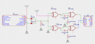
I added the XOR gates like in that schematic i sent, but unfortunately it doesnt work.
The output voltage becomes super unstable, it continues to go up and down. It peaks at more than half Vin.
But something is wrong...... What could be wrong!? I cant understand...
I used C 1nF and R 1K
Here is the schematic again:
Important: The outputs are actually flipped.
The upper XOR gate goes to pin 12 of ir2111 and the lower one to pin 10.
Attachments
Maybe unstable feedback. To exclude this, try manual duty cycle control. You need to make local feedback for error amplifier , and then add potentiometer from vref to gnd, and can adjust duty cycle manually. Output voltage would be unregulated, but voltage should be enough constant,to exclude instability. At moment can't tell which pins needs to be shorted, but i did that with this ic and with 494 too.
Its already in that mode. The duty cycle is constant at around 90 - 95%.
Maybe too high duty cycle?
Maybe too high duty cycle?
Ir2110 can't work at 100 percent dutt cycle without external power supply for high side. Bootstraps not works, because there's not enough time to charge capacitor when low side mosfet is on.
Its not 100% it is most likely 90% because the typycal maximum duty cycle for sg3525 is 45% per channel. Worst case around 47.
I will try to lower it to 85% and see if it solves the problem.
I will try to lower it to 85% and see if it solves the problem.
Well i tried but it still does not work. I managed to lower the output voltage but when drawing more current the inductor starts to vibrate at a low frequency (Like 700Hz) and the efficency becomes horrible.
Maybe this solution does not work......
Its a shame but thats where it ends, i guess.
I'm not ready to design DC-DC converters properly.
Maybe in the future........
Maybe this solution does not work......
Its a shame but thats where it ends, i guess.
I'm not ready to design DC-DC converters properly.
Maybe in the future........
Maybe feedback issue causing that 700 hz buzz. Try to manual pwm duty cycle method and check if this buzz would be still present.
You need to connect it's error amplifier as voltage buffer, and then supply a voltage from potentiometer 0-5v vref. The same can be done for tl494.
For SG3525 pin9 is opamp output ,pin1 inverting input , pin2 non-inverting input (according datasheet). Just connect pins 9 and 2 together and potentiometer's viper to pin2 ,and potentiometer's other two pins to pin16 and pin12 .
Thank you, i'm gonna try it out soon.
Initially i thought that i had too low output capacitance.
So, while the circuit was on i added another 2200uF capacitor on the output and...
Something got damaged.
They are not the MOSFETs nor the mosfet driver, i think it is the SG3525.
How did that happen? No idea 😂
I will replace it, its easy because the ICs are on sockets.
If the circuit works properly with a fixed PWM, how can i solve the feedback instability? Maybe by simply modifying the value of the COMP capacitor?
If PID needs to be implemented...
I'm a fool in this kind of stuff 😅.
LOTS of math involved for bode plots. Integrators / derivators have to be added in the feedback path. Not easy stuff...
Some time ago i've built psu for charger, it was based tl494 and ir2110, mosfets in halfbridge combination, and rewinded atx transformer. Had several times mosfets blown, until discovered, that ir2110 is very very sensitive where from it gets ground. On pcb i've had long and wide -300v track, at one end was high side capacitors bank minus, at middle - board with mentioned ic's, and at other end low side MOSFET source pin. Also halfbridge had it's own decoupling capacitor very close to MOSFETs. Mosfets blown when psu was just started , even at 50w output . Problem was that driver ic needs ground routed from low side mosfet source, not from elsewhere. When i cut that track from board with ic's and put a wire to MOSFETs source pin, no more blown MOSFETs. So check your layout carefully, if it follows datasheet layout, because this ic (ir2110) has it own limitations.
- Home
- Amplifiers
- Power Supplies
- Driving IR2110 with SG3525 for a synchronous buck converter