Kostas the pleasure is mine.
A very good software (REW) can make a dumb monkey look like a smart monkey if only he finds the right buttons to push.
But a very good software can't polish a turd.
Besides having built yourself a very good piece of test instrument, you have demistified the black box that a soundcard is (was) to some of us.
George

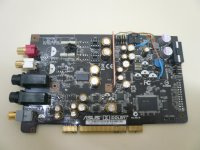

I love it! (what is at the third photo?)
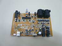
The question is why didn't you transplant the whole audio codec+ digital part (USB receiver ect) from the Behringer to your sound card but you chose to do it the hard way instead (build from scratch)?!
George
The question is why didn't you transplant the whole audio codec+ digital part (USB receiver ect) from the Behringer to your sound card but you chose to do it the hard way instead (build from scratch)?!
George
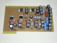
The question is plausible, and if If I understand correctly, @jp8 is going that way. 👍 Myself, I was really trying to find my way with all this back then and I was worrying about too many thin wires poking here and there. Actually, the audio codec chip was easy to include on my PCB. The big problem was the usb interface. Moreover, since I'm completely illiterate in code writing. First attempt was to transfer all parts from the Behringer to a new PCB hopping that the drivers would come together.😛 See attachment. A total failure... It reminds me to stay away from BGA chips. So, next step was a DIYINHK module and manual control.

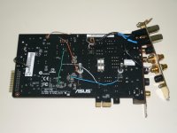
Third picture is an Asus essence STXII with power rails per section separated with a sharp cutter and connected to external regulators made to fit as a double slot PCI card. This project took another route leading to my DAC.
Third picture is an Asus essence STXII with power rails per section separated with a sharp cutter
and connected to external regulators made to fit as a double slot PCI card. This project took another route leading to my DAC.Attachments
What a beautiful pcb you've designed!
What's the BGA IC there?
Was the "failure" of software origin (drivers) or hardware issues?
The other pcb -the PCI card-is full of CLC filters and v. regulators. Are all these transfered to your sound card?
What's the BGA IC there?
Was the "failure" of software origin (drivers) or hardware issues?
The other pcb -the PCI card-is full of CLC filters and v. regulators. Are all these transfered to your sound card?
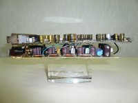
The BGA is the Xmos micro processor extracted from the Behringer soundcard together with all its peripherals. I struggled to reverse engineer the PCB to no avail and I had to follow the application notes of that chip. Either it was somewhere there I messed up or I wasn't lucky soldering the chip itself. It never came to life.
Regarding the other soundcard, if I understand correctly your question, the regulators' PCB is connected with wires to the Asus PCB as shown in post#102. It was a useful expirement about the effect of separate psu for each chip/block of the soundcard. This concept is applied to both my diy soundcard and my DAC.
Regarding the other soundcard, if I understand correctly your question, the regulators' PCB is connected with wires to the Asus PCB as shown in post#102. It was a useful expirement about the effect of separate psu for each chip/block of the soundcard. This concept is applied to both my diy soundcard and my DAC.
Dealing with BGAs takes a lot of courage. At least you tried. I wouldn't have tried that.Either it was somewhere there I messed up or I wasn't lucky soldering the chip itself. It never came to life.
Yes, that is what I meant. Transfer of the concept to your soundcard.It was a useful expirement about the effect of separate psu for each chip/block of the soundcard. This concept is applied to both my diy soundcard and my DAC.
The very clean noise floor is most probably due to these filtered multi PSUs.
The low THD at 0dBFS must be due to increased PSU voltage to the opamps (headroom).
These are the two technical strengths of your soundcard.
The third strong point is it's versatility.
Now the DAC must be another marvel of yours to test 🙂
George
By request, I post the diagrams for the front panel switches wiring.
The rotary switch that selects the preamp's gain is a 3pole/4pos. It takes 5V -from the usb Vbus, the ground goes to the I/O pcb relays "GND" pad. Then, pads P1, P2 and P3 are wired to the switch. Pictures and diagram below.


 The rotary switch that selects sampling rate is a 2pole/6pos restricted to 4pos. It takes M0 and M1 from the CS4272 and makes the combinations to ground and 3,3V from the usb module.


The "RESET" button was never found necessary so I think it can be safely omitted.
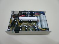
On other news, it was demonstrated that at least the input section can do its thing with humble LM78/79xx regulators. https://www.diyaudio.com/community/threads/behringer-umc-202hd-for-measurements.341309/post-6977625 So, I thought to redesign the PSU pcb to a much more cost effective version. Not tested! It still needs the mains to 5V converter but then it replaces the 5V to +/-15V converter and the 3,3V reg for the usb module. SIP4 DC/DC converters 5V in 15V out 3W is more than enough. Capacitors are whatever you can fit as low as 10μ, a few 1ohm resistors that form Pi filters and full three terminal regulators job. Attention should be paid for the two 3,3V regs marked with red color. In the market there is an alternative part LD33V with different pin out. I have provided extra pads to use all types. The one that stands upright is 3,3V/500mA for the usb module and it's meant to bend outside the pcb to attach to a heatsink. It should not touch the chassis.

The rotary switch that selects the preamp's gain is a 3pole/4pos. It takes 5V -from the usb Vbus, the ground goes to the I/O pcb relays "GND" pad. Then, pads P1, P2 and P3 are wired to the switch. Pictures and diagram below.
The "RESET" button was never found necessary so I think it can be safely omitted.
On other news, it was demonstrated that at least the input section can do its thing with humble LM78/79xx regulators. https://www.diyaudio.com/community/threads/behringer-umc-202hd-for-measurements.341309/post-6977625 So, I thought to redesign the PSU pcb to a much more cost effective version. Not tested! It still needs the mains to 5V converter but then it replaces the 5V to +/-15V converter and the 3,3V reg for the usb module. SIP4 DC/DC converters 5V in 15V out 3W is more than enough. Capacitors are whatever you can fit as low as 10μ, a few 1ohm resistors that form Pi filters and full three terminal regulators job. Attention should be paid for the two 3,3V regs marked with red color. In the market there is an alternative part LD33V with different pin out. I have provided extra pads to use all types. The one that stands upright is 3,3V/500mA for the usb module and it's meant to bend outside the pcb to attach to a heatsink. It should not touch the chassis.
Attachments
The ribbon connector from the audiocodec to the usb module is by far the most idiosyncratic feature of this project. I'll do my best to explain it. For starters, general info on how to make ribbon cables. Keep in mind that the ribbon cable holds repeated pairs of one signal and one ground wire.
Alas, in this case, things are so straightforward... The audiocodec layout does not match that of the usb module. The signal/ ground wires have to be rearranged. Below is a diagram, hardly meaningful and useless for different usb modules. Note that M0/M1 do not need their ground pairs.

The final implementation looks like this

Be prepared for trial and error and always check alignment, continuity and short circuits.
Alas, in this case, things are so straightforward... The audiocodec layout does not match that of the usb module. The signal/ ground wires have to be rearranged. Below is a diagram, hardly meaningful and useless for different usb modules. Note that M0/M1 do not need their ground pairs.
The final implementation looks like this
Be prepared for trial and error and always check alignment, continuity and short circuits.
Nice work, hats off.
Just thinking - the rate is selected by the USB host. The current rate signal should be available somewhere on the XMOS board (at least the leds connector? - I could not find any user guide for that board online).
Just thinking - the rate is selected by the USB host. The current rate signal should be available somewhere on the XMOS board (at least the leds connector? - I could not find any user guide for that board online).
Thank you very much!
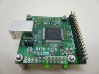
I don't have a user guide for the DIYINHK XMOS board either. Essentially, the pin out diagram posted above is all I could find. It came with a tiny OLED display supposed to show sampling rate, it should work but I never used it. It connects to the board with four wires. That's all I know. Is the logic pattern for M0/M1 universal, same for all converters? Or custom I2C needs to be implemented for each one? The later is beyond my skills, thus the rotary switch.
I don't have a user guide for the DIYINHK XMOS board either. Essentially, the pin out diagram posted above is all I could find. It came with a tiny OLED display supposed to show sampling rate, it should work but I never used it. It connects to the board with four wires. That's all I know. Is the logic pattern for M0/M1 universal, same for all converters? Or custom I2C needs to be implemented for each one? The later is beyond my skills, thus the rotary switch.
This picture shows LEDs indicating sample rate https://www.diyinhk.com/shop/696-la...dsd256-usb-tofrom-i2sdsdreclock-spdif-pcb.jpg , connected to a 6-pin section on the XMOS board. Your board seems to have a similar 6-pin section. IMO the manufacturer should provide the info on samplerate indication, did you ask DIYINHK?
Stand-alone mode selection in CS4272 (M0/M1) is related to samplerate ranges so DIYINHK LED indicator would not work directly. The original XMOS in Behringer may have used software mode instead (I2C).
Actually I did not mean a direction connection from the LED board to M0/M1, but perhaps a trivial OR logic (e.g. with diodes) could do.
I had purchased the usb module a few years ago and now it seems the model has been updated but it should be similar to this
https://www.diyinhk.com/shop/audio-...8ch_out_8ch_in_spdif_out/141-fifo_option-null
If I understand correctly, it has a new clock, a C-type usb connector and now instead of the OLED display it comes with LED indicators. Still, some basic logic is required. The best I could do is Diode/Transistor Logic like this https://www.diyaudio.com/community/threads/diode-transistor-logic-display-for-wave-io.371967/latest
But I think this would be even more steampunk technology than the switch. 🙂 Anyone who could provide a simpler solution is welcome.
The logic for LED-for-every-samplerate -> M0/M1 combination would be trivial - each samplerate (led signal) contributes either to M0, M1, or both, as specified in the datasheet table - diodes can do that easily.
After the psu revision I'm thinking for a revision of the digital converter board as well. CS5381-PCM1794 chipset... It could have auto sampling rate after all! I don't know when it will happen.
I had no response from DIYINHK about this. I sniffed around this 6-pin section in my module. Definitely no direct LED drivers there, so the reasonable thought is that it provides some signal that gets decoded on the LED pcb. Once we have the decoded signal driving each LED the rest should be very easy. A simple network of 1N4148 diodes to set M0 and M1 to "1" and two pull down resistors to keep them to "0". Thank you very much for pointing this!This picture shows LEDs indicating sample rate https://www.diyinhk.com/shop/696-la...dsd256-usb-tofrom-i2sdsdreclock-spdif-pcb.jpg , connected to a 6-pin section on the XMOS board. Your board seems to have a similar 6-pin section. IMO the manufacturer should provide the info on samplerate indication, did you ask DIYINHK?
Nice circuit. As of the LEDs, I cannot read the IC type, but it could be some binary -> decimal decoder - 4 bits + Vcc + GND. It should be quite easy to check the signals on the 4 data wires as seen on the LED board picture).
- Home
- Design & Build
- Equipment & Tools
- DIY soundcard intended for measuring amplifiers