I had a look at your SilentSwitcher when I was working on the the psu. It would be a very elegant solution indeed! But according specs, it delivers 150mA which is marginal if not low for this project. Two of them -and complete redesign of my psu- would be needed but then again, it would call for three usb ports together with the XMOS module. Nevertheless, thank you very much and I'll keep it in my mind as a last resort.
For now, I'm thinking to take the transformers and mains switch at a distance out of the chassis to check this factor. I'll report results.
For now, I'm thinking to take the transformers and mains switch at a distance out of the chassis to check this factor. I'll report results.
OK. Just let me know if you want to try it. And I think 200mA would not be a problem.
And there are USB chargers and Powerbanks with high charge current that can easily supply more that one SS.
For one of my units I have one of those new Powerbanks that can supply 9V or 12V as well, that will almost double the SS output current.
Jan
And there are USB chargers and Powerbanks with high charge current that can easily supply more that one SS.
For one of my units I have one of those new Powerbanks that can supply 9V or 12V as well, that will almost double the SS output current.
Jan
Last edited:
IIRC, USB has also a 50 or 100 Hz transaction frequency,
so that could also be the source.
(too tired to read the entire thread right now.)
so that could also be the source.
(too tired to read the entire thread right now.)
Last edited:
I'm wondering whether your input clamping circuit is part of the problem. Back to back zenners to ground instead maybe?
Tony.
Tony.
Whatever it is, it showed up when the opa1656 was inserted. The opa1632 was tested alone previously with the same psu and input scheme and layout -see post #29. I come to think that the differential input of opa1632 was canceling a lot of common mode noise... I'm planing to take FFT of the regulators' outputs. I'll let you know.
Just to clarify, do you mean an oscillation at the signal inputs or at the regulators? Sometimes, not periodically, I get a sign of oscillation by means of a "heart beating" FFT if my expression helps.
These are particularly difficult to find. It could be either. My guess would be to start with the last change, which I understand to be the opa1656. I would insert series resistances between it and the next stage or any of another things to look for. Power supply bypass not going to where it works best, input Z causing the input circuit to oscillate. There are lots of possible places to look. You need a wideband sensitive scope and isolate the probes with 100 Ohm resistors or they can kill the oscillation when you are probing.
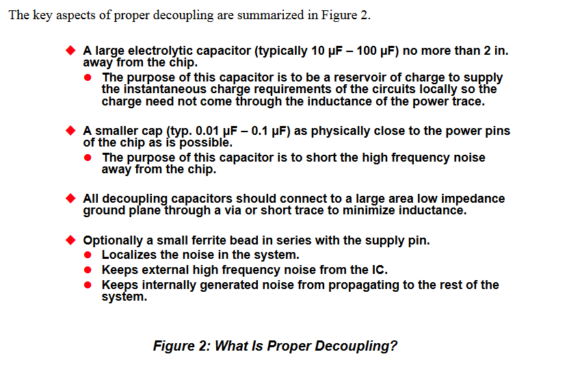
Actually going back and looking at the schematic, you have 0.1uF bypass on the opa1656 but no local resivoir caps. 100uF on each of + and - perhaps?
See below from Analog Devices app note on proper decoupling of opamps. https://www.analog.com/media/en/training-seminars/tutorials/MT-101.pdf
Tony.
See below from Analog Devices app note on proper decoupling of opamps. https://www.analog.com/media/en/training-seminars/tutorials/MT-101.pdf
Tony.
Attachments
I forgot to say that a second psu is required for the XMOS and this is 3,3V/800mA. This should be included in an off line solution since the XMOS does not provide galvanic isolation. Everything is on the table now.OK. Just let me know if you want to try it. And I think 200mA would not be a problem.
And there are USB chargers and Powerbanks with high charge current that can easily supply more that one SS.
For one of my units I have one of those new Powerbanks that can supply 9V or 12V as well, that will almost double the SS output current.
Jan
Unfortunately I haven't an oscilloscope at all... I'm trying with very simple equipment. But I will look at your suggestions.These are particularly difficult to find. It could be either. My guess would be to start with the last change, which I understand to be the opa1656. I would insert series resistances between it and the next stage or any of another things to look for. Power supply bypass not going to where it works best, input Z causing the input circuit to oscillate. There are lots of possible places to look. You need a wideband sensitive scope and isolate the probes with 100 Ohm resistors or they can kill the oscillation when you are probing.
The psu was designed from the regulators point of view i.e. LT3042/LT3094 app. notes. And these are located very close to the chips they supply. But this is just what I thought it will work...Actually going back and looking at the schematic, you have 0.1uF bypass on the opa1656 but no local resivoir caps. 100uF on each of + and - perhaps?
See below from Analog Devices app note on proper decoupling of opamps. https://www.analog.com/media/en/training-seminars/tutorials/MT-101.pdf
Tony.
I've been sniffing on the psu last night. I took some FFT using another sound card. Trying to set up all this I found something interesting. While the XMOS psu -a simple LD33V regulator feels fine floating from gnd, the main psu with the LT3042/94 regs -the bottom deck- was very upset while taking these measurements if not grounded to chassis/mains PE. I need to see why is this happening. I'll be back.
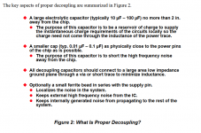
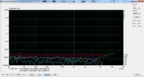
I'm getting there... slowly. The attached FFT shows the target when a couple of issues are addressed. One is solved! It was a ground loop. The metal chassis is earthed to mains PE, first thing done. The circuit gnd is not connected to the chassis to avoid ground loops when a DUT is connected. So far so good. But then there were the potensiometers' shafts. Grounding them became a necessity when the opa1656 came in allowing for much higher input impedance than the opa1632. Since they had physical contact to the chassis, I left them to mains PE rather than the circuit gnd. That was a bad idea. I took them to the nearest point of the ground plane and insulated from chassis with nylon washers. This killed a lot of noise! Also, I shielded the pot body with copper but I'm not sure it does anything. All this helped to reveal a lower level of noise coming from the transformers/mains wiring. The FFT was captured with all this stuff taken out of the chassis as long as the wires allowed. I have the impression that the culprit is the mains inlet and the wires to the transformers' primaries. I'm going to play around this the following days. It would be very handy if I could keep it mains psu.
Attachments
A few issues I can spot:
1. Pot tracking can ruin your input CMRR. Not good.
2. If you want to be avoiding ground loops under all circumstances, I'm sorry to say you would have had to use I2S galvanic isolators and separate input + ADC / output + DAC sections each with their own mains xfmr or other means of providing galvanically isolated power. (And then there still is mains xmfr primary-secondary coupling capacitance to contend with, several hundred pF even on a smallish part. I don't think they make very many small ones with a shield winding, <20 VA usually is OK as-is but it can be a real issue up in the hundreds of VA and needs to be taken care of in integrated / power amps.)
3. Mains pickup from the primary section could be either electrostatic (-->apply shielding, run mains wire next to chassis) or inductive (--> identify loops in signal path and reduce loop area to a minimum via layout - usually that means keeping signal conductor pairs next to each other at all times, including any Ts like the ones for your bulbs, which ultimately may become an Achilles heel).
Last edited:
All good advice and much appreciated! Obviously, things can get insane for a no compromise design. But then, my limitations come into the game. For example, a better digital converter most likely would require I2C control port and that is simply beyond my handling... So, starting from something I could use and keep it within my budget, it could only be just descent at best. In other words the CS4272 sets the limits in this design and apparently the analog circuitry around it is tracking well.
At some early point I made thoughts about galvanic isolation. Although it seems easy, it requires reclocking and I put it aside. Searching for all this, I found that there is no electrical continuity between usb ground and PC chassis/mains PE. Meaning that usb can pass a lot of digital hash but is not responsible for ground loops(?) Indeed, my findings are pointing to this direction. The low frequency noise is more like what you describe in the third section of your reply.
The input attenuator/buffer took the most of my effort. Not meaning the best it could be done... I realize it can take a lot of improvements for the very best loop measurements. But what I needed was a handy tool. So, even if a stepped range selector is used in front of the ADC, there must be a potensiometer somewhere in the test set up anyway. This is where I think the low cost rigs suffer. The motivation behind this project was to build a device ready to use, plug in a rough prototype and have it measured. It's not intended to compete the top class bench equipment. It takes it from the soundcard point of view, the weak link.
I had a break from diy action these days. Happy New Year to everyone!
Last edited:
Finished!
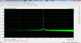
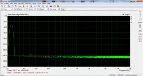
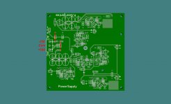
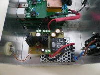
The toroid transformer's magnetic shield works really good eliminating 50Hz interference but there was another problem. A tiny 100Hz peak barely seen on the noise floor yet waiting there to get excited by anything around it. Something to do with the center tap/rectifiers obviously. Anyway, trying to stay with plan A -one box, one power cord- I replaced the transformer with SMPS. I used MeanWell for availability and cost. One RS-15-5 from mains to 5V/3A DC and then split to a linear 3,3V reg for the XMOS and a DKM10E-15 to boost at +/-15V. The reservoir caps on the psu deck cannot stay as they exceed the max load capacitance of the DC converter by a lot. I left on 220μF per rail. And the input takes 47μF because this was mentioned for the RS-15-5. See pic for the conversion of the psu. Just bridge D3 and D4. Pcb for the SMPS is not mandatory but I made one and gerber files are attached. Lay out is for LD33V which is different from LM78xx series.
Everything works a charm, tested with real DUTs as well. Now it gets seal of approval!
Attachments


Very nice, congrats!
Would you be interested in providing boards, parts, kits, or even a finished box?
Would you be interested in providing boards, parts, kits, or even a finished box?
Thanks! Sorry, I can't support anything like that at the time being. But with all info provided, everyone could build his own.
Did you figure out the issue with the 44 kHz limit?
It's not going to be any better because of the audio codec chip. Actually it's a feature of all digital converters. The bandwidth is deliberately limited for better noise performance in the audio band. For CS4272 the limit is around 44kHz.
- Home
- Design & Build
- Equipment & Tools
- DIY soundcard intended for measuring amplifiers