Thanks for schematic and gerbers @schultzsch - it's good of you to share your work. Your schematic shows a sjep120r100 but it looks as though you used a Tokin (THF-51S ?) in your actual implementation - does using the Tokin imply any other component changes to the schematic? Apologies for my basic questions but I don't possess your electronics expertise so I can only follow the lead of others like yourself.

The others around are sharing their work too so I am following them..
No changes needed from component pov. You adjust the vds as needed. In my case I set the power supply to 30v and settled with ~15.6vds on the 2sk182es(this is what I use)
I have a pair of jfets from Pa and one day I will try them too but not too soon.
No changes needed from component pov. You adjust the vds as needed. In my case I set the power supply to 30v and settled with ~15.6vds on the 2sk182es(this is what I use)
I have a pair of jfets from Pa and one day I will try them too but not too soon.
Thanks a lot @schultzsch for sharing all the goodies, schematic, Gerbers (PCB ordered) and BOM, I’ll practice my SMD soldering skills 👍
It is greatly appreciated.The others around are sharing their work too so I am following them..
I’ve had some more fun today.
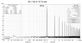
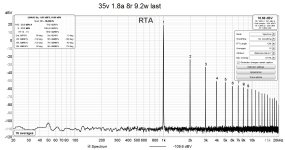
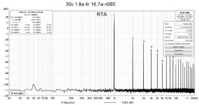
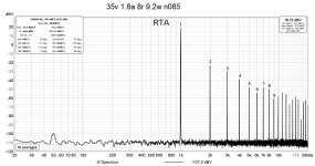
I replaced the irfp150 in the ccs with ixfn280n085. I have lots of these pucks and the curiosity of trying them was huge.
At low power(1w) the results are very close the difference starting to creep in at higher power levels, though not much. This at 1khz, at higher frequencies the difference will be bigger.
So my conclusion to all this is if I need more output power(which I don’t) and the dissipation on the irfp goes above 40-50w I have to resort to the big pucks with some penalty in thd.
Attachments
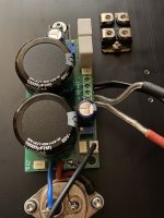
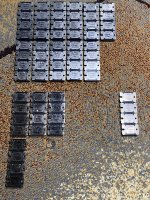
If there is anyone who wants to build this amp with higher rails and higher bias I can offer a few pairs(of pucks)for just only the shipping cost.
I am back 🙂
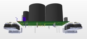
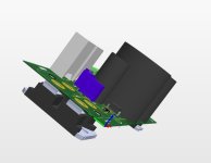
Yesterday I decided to match for vgs all my puck mosfets. I got a few quads so this gave me the idea to make a new pcb to accept the pucks(if needed also the to247 mosfets).
With this pcb you could build a full mos follower needing 4 pucks or vfet/mos needing only 2 pucks.
I have more than 10 quads of matched pucks and was thinking that if there is enough interest I can give these for cheap together with the gerbers for the pcb so you can build the amp. I can divide them also in matched pairs.
You can argue that matching is not needed but I did it to be able to have close min/max currents when adjusting the ccs and hopefully close transconductance for the gain devices when going mos/mos.
What do you think?
Attachments
Last edited:
Very nice work 👍
Since I already ordered some PCB of your original PCB can the originale one be used for both type of amplifier, meaning MOSFET/VFET and MOSFET/MOSFET ? Or, is there components that are different or added between the 2 configurations?
BTW, I wonder if these MOSFET puck need a thermal pad ? Spec sheet doesn’t seem to say if Source or Drain is connected electrically to the case underneath.
Eric
Last edited:
Thanks Eric
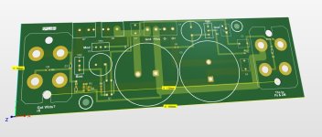
Yes both pcbs work with mos/mos or vfet(or jfet)/mos.
If you want to use the pucks with the older pcb you will need to use wires for the connections.
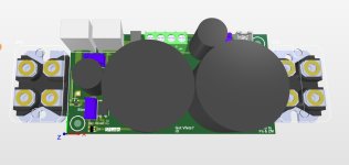
The pcb for the smaller irfp mosfets works only up to 45v.
This one is able to go higher, has an extra zener in series with the ccs.
The pucks need lower gate resistors than the irfps. At ZM’s suggestion I will add some series ferrite beads together with the resistors.
Also I have to add pads for the vfet at the suggestion of nautibuoy.
No thermal pad needed for electrical isolation.I dissipated ~120w/device without even adding thermal paste. Well now some thermal paste you can add in there 🙂
Yes both pcbs work with mos/mos or vfet(or jfet)/mos.
If you want to use the pucks with the older pcb you will need to use wires for the connections.
The pcb for the smaller irfp mosfets works only up to 45v.
This one is able to go higher, has an extra zener in series with the ccs.
The pucks need lower gate resistors than the irfps. At ZM’s suggestion I will add some series ferrite beads together with the resistors.
Also I have to add pads for the vfet at the suggestion of nautibuoy.
No thermal pad needed for electrical isolation.I dissipated ~120w/device without even adding thermal paste. Well now some thermal paste you can add in there 🙂
Would be nice to have a dedicated thread about the @schultzsch amp with all its specific documentation and discussion.
That wouldn’t be a problem once I have the pcbs and a built prototype(with the actual pcb), most probably in January.
If I drew a pcb for it doesn’t mean it’s my amp. It’s still Pa’s, I only adapted it for my greediness 🙂
If I drew a pcb for it doesn’t mean it’s my amp. It’s still Pa’s, I only adapted it for my greediness 🙂
You are right but maybe some that don’t have time to look up daily for hot sales in the swap meat section of the forum for the vfet kits or the vfets have already the tokin ones and want to build something similar.
Btw did you get to build something with the vfets in the earlier post or with the others that you already had?
Btw did you get to build something with the vfets in the earlier post or with the others that you already had?
Decisions, decisions,... I hope to make up my mind soon. 😏did you get to build something with the vfets in the earlier post or with the others that you already had?
- Home
- Amplifiers
- Pass Labs
- DIY SONY VFETS pt 3 - Got VFETs?