Gerbers for a mini group buy would be ideal, with a BOM list. I have the VFETs available and ready to use.
Yes,could the gerbers be made available. I have a couple of 2sk60 that I would like to put to use.
One issue to consider is whether the TO-3 IRF250 (or an adequate replacement) is available from reliable sources.
I have lots of those, and brackets to mount them on the UMS sinks in the store.
If there is demand I could make them available.
If there is demand I could make them available.

Any movement on stocking more PCBs in the store, or providing the gerber files?
I'm taking a PCB design class at a local community college starting in July. Maybe I can make a layout as part of the class using the article layout as a guide. (With a little lot help from folks on the forum)
I'm all for bringing the kits back for a triumphant 2024 summer reunion tour if the parts are available.
I'm all for bringing the kits back for a triumphant 2024 summer reunion tour if the parts are available.
It's a little disappointing that there has been no response to the various requests for PCBs or Gerber files to build more of the Sony VFET amps - I have a pair of 2SK60 VFETS and the necessary MosFets I would like to use.
The PCB is actually pretty simple so I think I'll start laying out my own PCB design, referenced to Nelson's original article on the design.
The PCB is actually pretty simple so I think I'll start laying out my own PCB design, referenced to Nelson's original article on the design.
You can also use proto boards, or perf boards, or strip boards with great success as this circuit is simple enough to allow this.
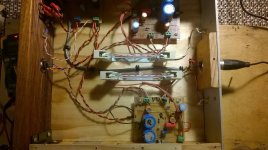
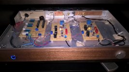
Some years ago I built in succession ZenLite Headamp, Pearl 1 Phono and MoFo with strip boards and they are still going strong without hiccups.
In the photos below the 1st one is Zen, the next Pearl.
Some years ago I built in succession ZenLite Headamp, Pearl 1 Phono and MoFo with strip boards and they are still going strong without hiccups.
In the photos below the 1st one is Zen, the next Pearl.
Attachments
In my amps with 2SJ18 I don't use a front-end and I have one transformer input. Is it possible remove the C4 input capacitor?

There is a DC bias voltage at the gate of the VFET which the capacitor blocks.
Hello Nelson,I have lots of those, and brackets to mount them on the UMS sinks in the store.
If there is demand I could make them available.
If we make a list of those who want to participate in this special group buy could you tell us how to pay and give our addresses? Or just tell us to set up a GB and have one of us do the shipping and ordering process. At the end you send the whole shipment to the GB organizer to deal with it. Or any other way that is easy for you.
Just a pity that they are in your storage and we would love to buy them....
All the best,
Leo
Ps nearly Christmas 😇
Many thanks, I was hoping the input transformer could perform the same workThere is a DC bias voltage at the gate of the VFET which the capacitor blocks.
I have a P kit and a while back started making a board for the N channel. I used my P board to get the sizes for the board, caps, resistors, hookup pads, tracks, etc. I then just copied the layout diagram from the diy sony vfet os-2 pdf pictures - (https://www.firstwatt.com/wp-content/uploads/2023/12/art_diy-sony-vfet-os2.pdf)


But I got stuck because of R9 - on the board diagram the "left" side of R9 is hooked up to ground but in the schematic it is between the out + and out - ?
I think the board/layout diagram may be wrong but then going through the pictures of actual boards from threads its very hard to tell. I also searched them for any mention of changes or an error but couldn't find any (probably because its my own error somehow).
Here is a pic of my layout so far with R9 circled. For now, I went ahead and hooked it up to OUT- instead of Ground, following the schematic, but I could very easily be (and I probably am) mistaken. Thoughts?
In my opinion, R9 in the schematic of #558 is just a "bleeder" resistor, whose job is to discharge C1 and C5 when the DC power supply is disconnected and/or when there's no music signal for a long period of time. It also handles the situation where C1 or C5 has a little bit of DC leakage. Yes, Virginia, real world capacitors do have a wee amount of DC leakage, they're not perfect open-circuits at DC. Especially big ole bohunker electrolytic capacitors.
In my opinion it doesn't matter whether R9 is connected between "+O" and "-O" as shown on the schematic, or whether R9 is connected between "+O" and "GND" as shown on the layout. The total bleed resistance is either 1000.47 ohms, or 1000.00 ohms. Not anything to worry about, no sonic impact at all, do whatever makes your life easier. But please make the schematic match the layout, whichever choice you make. That way Future-You won't discover they are different, and forget why Current-You did such a confusing thing, and also forget whether that's truly an issue or not.
In my opinion it doesn't matter whether R9 is connected between "+O" and "-O" as shown on the schematic, or whether R9 is connected between "+O" and "GND" as shown on the layout. The total bleed resistance is either 1000.47 ohms, or 1000.00 ohms. Not anything to worry about, no sonic impact at all, do whatever makes your life easier. But please make the schematic match the layout, whichever choice you make. That way Future-You won't discover they are different, and forget why Current-You did such a confusing thing, and also forget whether that's truly an issue or not.
Bleeder resistor, thanks Mark, I figured it was something I didn't "see" or understand but that makes perfect sense when I look at it again. Not connecting it to the OUT - just takes out the loop around the board through the 0.47 R. "Shorter" path. Greatly appreciated.
If it won't change anything functionally, I think I will just leave it as I have it. Like you said, if I ever had an issue or something I would just look at the schematic in the pdf from the web. Thanks for the tip and insight.
If it won't change anything functionally, I think I will just leave it as I have it. Like you said, if I ever had an issue or something I would just look at the schematic in the pdf from the web. Thanks for the tip and insight.
- Home
- Amplifiers
- Pass Labs
- DIY SONY VFETS pt 3 - Got VFETs?