Hi All,
I posted earlier that I have readable schematic for this NAD 3240PE. I am happy to share that, if anyone want a copy.
Now I have to try to solve the problem - the right channel doesn't respond to the balance adjustment as it should.
The amp sounds very nice, completely noise free when nothing is playing. IF I turn the balance knob all the way to the right and then just a little left to get some left channel going I can turn it up and get very pretty sound, but the right channel has only a tiny fraction of the left channel power.
If I take the Pre Out to another amp it sounds just fine, but when I use the integrated amp not much right channel.
I am surprised by this, I would have expected the balance pot to be a preamp failure, not manifested by the power amp alone.
I tried the usual contact cleaner hose out and rotate business. No difference.
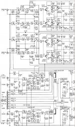
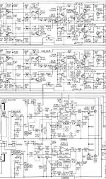
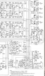
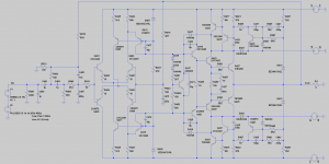
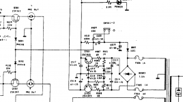
I am attaching images of the schematic (the rest of the service manual has component lists, wiring diagrams, etc.) that can be placed side by side.
I probably just don't understand how the switches and pots work together and all I need is a new balance pot, but I could use any trouble shooting advice you all are willing to share. Should I go for a volume pot, too - while I am in it?
Thanks! BentMike
I posted earlier that I have readable schematic for this NAD 3240PE. I am happy to share that, if anyone want a copy.
Now I have to try to solve the problem - the right channel doesn't respond to the balance adjustment as it should.
The amp sounds very nice, completely noise free when nothing is playing. IF I turn the balance knob all the way to the right and then just a little left to get some left channel going I can turn it up and get very pretty sound, but the right channel has only a tiny fraction of the left channel power.
If I take the Pre Out to another amp it sounds just fine, but when I use the integrated amp not much right channel.
I am surprised by this, I would have expected the balance pot to be a preamp failure, not manifested by the power amp alone.
I tried the usual contact cleaner hose out and rotate business. No difference.
I am attaching images of the schematic (the rest of the service manual has component lists, wiring diagrams, etc.) that can be placed side by side.
I probably just don't understand how the switches and pots work together and all I need is a new balance pot, but I could use any trouble shooting advice you all are willing to share. Should I go for a volume pot, too - while I am in it?
Thanks! BentMike
Attachments
It uses NAD's power envelope (as in PE) technology to get more peak power from a basic design at lower cost than simply build a bigger amp. The scheme works well and sounds good according to owners but for the average DIY, is one son of a gun to troubleshoot. Don't rush into this like it's just another amp.
")
Glad it is useful. Wish I had the tools to sort mine out. It is still a shelf stabilizer.
I apologise profusely for not actually reading your request for help and just grabbing the schematics you posted.
From the sounds of it there's something going on with either the right preamp output or else the right power amp input.
Divvy up the problem by trying another preamp on the power amp, then trying a different power amp on the pre.
I'm guessing here, but if there's no obviously smoked transistors that are the culprit I'd be looking at leaky electrolytics in the right channel power amp - starting with C410...
Another possibility is C416. This is supposed to ensure the amp has unity gain at DC, but gain set by R444 & R476 at AC. Ignore the stuff after R446 - that’s just to provide DC offset adjustment from the look of it. Anyway if C416 goes open then the AC gain will drop from ~20 back to 1 and the amp will be really quiet.
The receiver version manual for NAD 7240PE is a lot clearer and contains the power amplifier schematic on a single page. Free download after signing up here: NAD 7240PE - Manual - Stereo Receiver - HiFi Engine
Okay - here 'tis without the soft clipping gumph at the input and without the PE stuff. I used TIP3055 & TIP2955 models for the output pair as I couldn't find models for the 2SD1047 & 2SB817, and figured they're probably not dissimilar to a 3055/2955.
The models I did find are as follows:
.model 2SC2240 NPN (IS=9.98557f BF=444.22 NF=965.739m VAF=439.144 IKF=99.567m ISE=6.48962f NE=1.29179 BR=425.865m NR=1 VAR=0 IKR=954.972 ISC=539.648p NC=2 NK=500m ISS=0 NS=1 RE=0 RB=0 RBM=0
+IRB=0 RC=168.128m CJE=2p VJE=750m MJE=500m CJC=11.7089p VJC=750.026m MJC=499.123m XCJC=1 CJS=0 VJS=750m MJS=0 FC=500m TF=1.41635n XTF=499.995m VTF=10 ITF=10.055m PTF=0 TR=10n EG=1.11 XTB=0 XTI=3 KF=0 AF=1
+Vceo=120 Icrating=100m mfg=Toshiba)
.model 2SA970 PNP (IS=9.9855f BF=477.115 NF=965.739m VAF=64.7 IKF=116.959m ISE=2.13187f NE=1.27276 BR=385.069m NR=1 VAR=0 IKR=308.018 ISC=13.4194p NC=2 NK=500m ISS=0 NS=1 RE=0 RB=0 RBM=0
+IRB=0 RC=7.03858 CJE=2p VJE=750m MJE=500m CJC=19.119p VJC=749.982m MJC=498.685m XCJC=1 CJS=0 VJS=750m MJS=0 FC=500m TF=1.49138n XTF=500m VTF=10 ITF=10.0655m PTF=0 TR=10n EG=1.11 XTB=0 XTI=3 KF=0 AF=1
+Vceo=120 Icrating=100m mfg=Toshiba)
.model 2SD669 NPN (IS=5p NF=1 BF=250 ISE=5p NE=1.5 IKF=3 VAF=150 RB=1 RC=0.25 RE=0.25 TF=1.14ns CJC=50p )
.model 2SC3423 NPN (IS=14f BF=130 VAF=50 IKF=300m BR=5.61 VAR=500 RB=10 RE=0.01 RC=0.8 CJE=5p VJE=0.7 MJE=0.5 TF=795.77p XTF=7 VTF=6 ITF=50m
+CJC=4.4p VJC=0.6 MJC=0.286 XCJC=0.5 TR=4n XTB=1.5 EG=1.11 XTI=3 FC=0.5)
.MODEL 2SA1360 PNP (IS=116.73f BF=147.48 VAF=100 IKF=78.684m ISE=297.72f NE=1.5511 BR=.77363 VAR=100 IKR=1.0217 ISC=26.92n NC=2.9970 NK=.49889
+RC=4.5038 CJE=4.0176p MJE=.33333 CJC=6.287p VJC=.35 MJC=.26272 TF=344.39p XTF=84.382 VTF=7.0050 ITF=.11443 TR=10n)
Anyway it seems to work reasonably well - 0.003% pushing 1KHz, 28V RMS into 8Ω. Dunno why they bothered with the PE stuff - the basic amp is quite nice.
Guess it all comes down to marketing in the end.
Attachments
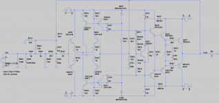
And with the PE stuff added - excuse the transistor substitutions.
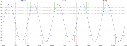
I can see why they did the PE stuff now - it makes for a very capable amplifier with low quiescent - assuming the driver SOA and supply are looked after, it will push an easy 240W into 8Ω.
The graph says it all about the PE - it's a straightforward class H - n010 and n040 are the collectors of the main driver transistors.
Bear in mind the specs for this thing say "40W RMS into 8Ω". That's an impressively conservative rating.
Attachments
Oh that's a doddle. There are two ways to do it - a low power version and a high power version.
For the low power version, remove the PTC thermistors PTC1 and PTC2. Now the amp will be a conventional Class AB running off a 43V supply.
For more fun:
Remove PTC1 and PTC2, and replace them with wire links.
Remove Q431, Q432, Q433 and Q434. Add wire links between the collector and emitter of each. This turns PE on permanently, putting 71V on the collectors of the main output transistors.
Remove Q427, Q428, Q429 and Q430, and replace with something that's a tad more capable. 2SC5200 & 2SA1943 should do well here, with improved Vceo (230V vs 140V, improved Ic (15A vs 12A), improved Pc (150W vs 100W) and otherwise similar to the 2SD1047 and 2SB817.
Replace the heatsink with something that's not a folded bit of tin, as the quiescent power consumption will have gone up rather a lot. I reckon a Conrad MF30 series should do the job well (Conrad Heatsinks - Products).
It'll need rebiasing, as the Iq will have changed with the different output devices.
Now it's a class AB running off +/-71V supplies, and is solely limited by what the power transformer will supply.
A larger power transformer and heatsinks are sure needed for the high power option but how to mount them? To keep it simple, I'd take the lower power option as it's less hassle and I'm fairly sure that even in the basic 40W/8R mode, sound quality would be not be significantly affected and power adequate, at least for many NAD users.
I haven't seen any explanation of their failure modes but it seems to be a common characteristic once this amplifier type is in use for around 20 years. I saw a number of them turning up at recycle plants in my region back then, which may suggest bad PCB soldering or caps. However, there was likely more serious damage as a result, which ended in scrapping rather than repair.
I haven't seen any explanation of their failure modes but it seems to be a common characteristic once this amplifier type is in use for around 20 years. I saw a number of them turning up at recycle plants in my region back then, which may suggest bad PCB soldering or caps. However, there was likely more serious damage as a result, which ended in scrapping rather than repair.
Last edited:
Cool - glad I could be of some help.
I have a 3240PE winging it's way to me as I type - I'm really looking forward to playing with it. I admit that a significant motivation for buying it was that it's got the rectangular green power button and logo placement of all my other NAD stuff, whereas the power button on my 3020 is larger, black, and square, plus the logo is offset. That's about the most incredibly wrong reason to buy a new amplifier, but that's just me.
I have a 3240PE winging it's way to me as I type - I'm really looking forward to playing with it. I admit that a significant motivation for buying it was that it's got the rectangular green power button and logo placement of all my other NAD stuff, whereas the power button on my 3020 is larger, black, and square, plus the logo is offset. That's about the most incredibly wrong reason to buy a new amplifier, but that's just me.
My 3240PE arrived through the week, and I just got home to have a play. The output from the pre is down ~40dB from what it should be. One side of the power amp appears to work quite nicely, the other side is missing it's PE bit on the positive side - that's the weirdest clipping I've ever seen (note it's divide by ten).
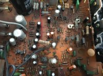
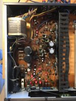
Oh, and it's filthy. Bloody smokers. I think before I progress much further I'll give it a thorough wash.
Oh, and it's filthy. Bloody smokers. I think before I progress much further I'll give it a thorough wash.
Attachments
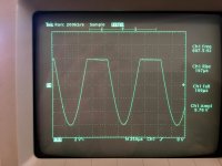
That looks pretty grubby! And an interesting waveform you've got there. Hope you can get that back on it's feet without too much trouble!
I just got hold of another 3020i to recon. I've found this one to be heavily molested by someone who has no right to be near a soldering iron... Blown traces, Q511 (BD139) soldered to thin air (quite funny), 4A fuses in the 1A holder, random other fuse values.. The list goes on.
But best of all, a lesson in using a bulb tester on initial turn on.. The PCB had not been put into the little tabs correctly and the live 100Vpp AC section was pressed onto the bottom of the case! (Perhaps explains the 4A fuses in the 1A positions...). Being double insulated, I suspect the case was live and waiting to bite...
Waiting for a pile of silicon to arrive next week so that I can replace the regulator section as well as one output channel that had been fried.
I'd be interested to hear what you find is causing your problems.
Part way through - I've sorted the pre anyway. I was getting a signal as far as the mute JFETs, but no further. The circuitry around the power-on muting circuit is significantly different for the 2340PE and the 7240PE (I spent twenty minutes searching for Q503 on the 3240PE circuit board before I figured that out. So the dodgy 3240PE schematic is luckily good enough.
Anyway it was very easy once I'd worked out the circuit. The JFETs are turned off when the power is off, by holding their gates at -30V. When you turn it on, C520 (4µ7 50V) charges slowly to +20V via R510 (680K), eventually turning the JFETs on. In my case C520 was a bit leaky, so it never charged up and never came out of mute. Replacing C520 fixed that.
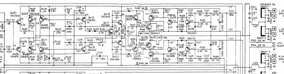
I'm suspecting one of the PE transistors for the lack of +70V drive for the left channel (possibly Q431) as I've definitely got +70V available at the +ve side of C453, and the cathode of D431 is driving up above 43V happily.
Anyway it was very easy once I'd worked out the circuit. The JFETs are turned off when the power is off, by holding their gates at -30V. When you turn it on, C520 (4µ7 50V) charges slowly to +20V via R510 (680K), eventually turning the JFETs on. In my case C520 was a bit leaky, so it never charged up and never came out of mute. Replacing C520 fixed that.
I'm suspecting one of the PE transistors for the lack of +70V drive for the left channel (possibly Q431) as I've definitely got +70V available at the +ve side of C453, and the cathode of D431 is driving up above 43V happily.
Attachments
And now it's working properly.
The lack of +70V drive on the left channel was due to a dead 2SB649, Q435. This is the transistor that turns the main HV switch on.
I don't have any spares for that, but while I was working I noticed that in a previous repair someone had substituted 2SB649 and 2SD669 transistors for Q419 & Q421. While this substitution clearly worked, they really aren't the right part for this spot. I noted that the other channel uses 2SC2911 and 2SA1209 here (original from factory from the look of it), so did a bit of swapping and ended up with a spare 2SB469, which then went into Q435.
So yay, all working nicely now.
I've also done some more capacitor replacement (everything bar the high voltage 100V and 80V ones which I don't keep stock of, and some 330µ 35V ones on the preamp supply which I also don't have in stock. So it's still a Mouser order from finished. I think I'll order new trimmers too, as the ones it came with are awful.
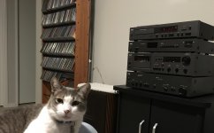
In the meantime it's gone into my NAD stack, and it's very nice to have matching logos and green power buttons finally. My cats are impressed.
The lack of +70V drive on the left channel was due to a dead 2SB649, Q435. This is the transistor that turns the main HV switch on.
I don't have any spares for that, but while I was working I noticed that in a previous repair someone had substituted 2SB649 and 2SD669 transistors for Q419 & Q421. While this substitution clearly worked, they really aren't the right part for this spot. I noted that the other channel uses 2SC2911 and 2SA1209 here (original from factory from the look of it), so did a bit of swapping and ended up with a spare 2SB469, which then went into Q435.
So yay, all working nicely now.
I've also done some more capacitor replacement (everything bar the high voltage 100V and 80V ones which I don't keep stock of, and some 330µ 35V ones on the preamp supply which I also don't have in stock. So it's still a Mouser order from finished. I think I'll order new trimmers too, as the ones it came with are awful.
In the meantime it's gone into my NAD stack, and it's very nice to have matching logos and green power buttons finally. My cats are impressed.
Attachments
- Home
- Amplifiers
- Solid State
- DIY includes repair? NAD 3240PE advice needed...