Hello ripblade,Don't most opamps operate in A/B?
most OPAmps can be biased into ClassA...
search the net:
https://www.google.com/search?client=firefox-b-d&q=opamps+running+class+A#ip=1
Cheers
Dirk
I'm aware, but how often is this done at a commercial level?most OPAmps can be biased into ClassA.
Not often.
BTW, I give credit to Barry Thornton of Quintessence who showed me that
trick back in '72.

BTW, I give credit to Barry Thornton of Quintessence who showed me that
trick back in '72.

John Curl used the same trick in his Parasound JC3 preamps. 2SK246Y JFET (constant current source) from opamp output pin to negative supply rail. Datasheet IDSS for the Y classification is 1.2mA to 3.0mA.
First I heard of it was in an article by Walt Jung. The LT1010 and LT1115 data sheets show it.
Hi,i want to try on a breadboard and i'm looking for the final as built schematic diagram.
Can someone help?
1)This will be used as preamplifier for F4. balanced to unbalanced option.
2)what is the purpose of R14 and what's the value?
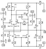
PS .Is this what i'm looking for?
Thanks in advance!
Can someone help?
1)This will be used as preamplifier for F4. balanced to unbalanced option.
2)what is the purpose of R14 and what's the value?
PS .Is this what i'm looking for?
Thanks in advance!
Attachments
Last edited:
See the post #686 by Nelson in this thread for all of your answers - and more on the latest revision. First iteration is in post #1.
In order to get the best noise performance in a jfet ips design you need large area jfets. I asked Scott Worcer this question a while ago? His answer was that very low noise jfets are large area devices, meaning that they are expensive to use for an opamp since cost is related to die size.But what is the advantage of using discrete transistors when chips such as OPA1642 have a Jfet differential input and very nice performances ?
This circuit don't love breadboard...
I used non matched for Q1,Q2,Q3,Q4.
CCS Q3=2.8mA
CCS Q4=8mA
I have tried R3,R4=22K
(gain2.2) and R3,R4=100K.(gain10).
Power supply is +22V regulated.
The breadboard test circuit oscillate in both gain leveles .
I used non matched for Q1,Q2,Q3,Q4.
CCS Q3=2.8mA
CCS Q4=8mA
I have tried R3,R4=22K
(gain2.2) and R3,R4=100K.(gain10).
Power supply is +22V regulated.
The breadboard test circuit oscillate in both gain leveles .
Attachments

Is virtual ground solidly 11V? If you've checked wiring, could try adding a BFC (100-1000pF) from Q5 base to collector or to VG. Also check DCV at Q5 base.
Also keep -IN grounded for now.
Also keep -IN grounded for now.
Thanks,i will try your suggestions soon.
Just now i have tried to connect between sound card and power amplifier,it is functional but with hum and worm power amplifier(oscillations).
PS.I have tried C6= 27-54pf but worse results.
Just now i have tried to connect between sound card and power amplifier,it is functional but with hum and worm power amplifier(oscillations).
PS.I have tried C6= 27-54pf but worse results.
Is virtual ground solidly 11V? If you've checked wiring, could try adding a BFC (100-1000pF) from Q5 base to collector or to VG. Also check DCV at Q5 base.
Yes,vg=11,4VAlso keep -IN grounded for now.
Q5 Vbe=0.6V
VR6(680R)=0,68V
What do you mean,keep -IN grounded?
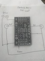
Eliminate C2 and R2 connected to 0V?
I use this configuration as in photo.
Attachments
Last edited:
Don't eliminate those parts; you're correct--just drive SE as you show, and not BAL. When you get it sorted out, you can use BAL, but easier for now to keep it simple.
I haven't used those breadboards in a long time. Maybe they're the problem, as william2001 states. ¯\(ツ)/¯ Does the oscillation change when you touch around the different nodes?
Maybe ZM needs to come knock our heads to get it fixed.
 🤔
🤔
I haven't used those breadboards in a long time. Maybe they're the problem, as william2001 states. ¯\(ツ)/¯ Does the oscillation change when you touch around the different nodes?
Maybe ZM needs to come knock our heads to get it fixed.
🤔- Home
- Amplifiers
- Pass Labs
- DIY Front End 2022