I seem to have stepped in it by suggesting that pin 1 of the transistor be marked. The point isn't that what's there now is unclear, the reverse side is very useful and I use it to test the transistors all the time. The point is to know the physical orientation of the part when installing it. I liked the square for pin 1 pad, which is what I'm used to on my boards. Other outlines have a little dot by pin 1. This is not intended as a criticism like what's there is wrong, because it's not wrong. It's just a suggestion that would make my work a bit easier, and perhaps some others. Logical function is not the same as physical orientation.
These boards are great! I just made a suggestion that might make them a little better for the manual assembly.
These boards are great! I just made a suggestion that might make them a little better for the manual assembly.
^ FWIW, I don't think you stepped in it at all.
My worry was/is that people would blindly stuff all parts in the same orientation w/o checking the actual pinout of the parts they specifically chose for their builds. I've done that ... and I hope to never repeat that error. However, I am still what would be generally considered a VERY novice builder.
Bringing up suggestions creates good conversations. Thanks for bringing it up.
BTW - No way in the world I can assist with your previously posted issue, but I'll be watching to learn what's determined.
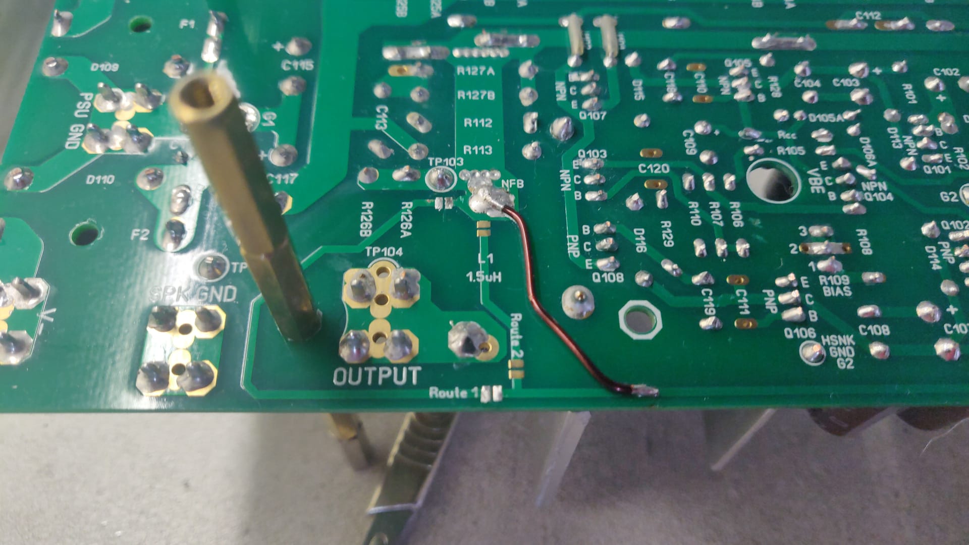
very good , I've already done this for the "mini". I actually had the more direct route for NFB , then KT wanted to loop it around the OPThis is another improvement, for both the EF3-3 and EF3-4 boards
traces. By having all this testng , no issue - I can pump out perfection !!
This was done on the "slewmaster" OPS.This is another improvement
First time. Badger , Slewmaster , and wolverine. Never had any oscillation , except for the "infidel" H- bridge IPS.I need some help from you folks. I am working on bringing up an EF3-3 board. I am at the point where J103 is installed and none of the output transistors. Other than that the build is complete.
During testing, I noticed a 6dB/oct roll off starting at 10kHz. I figured it was a cap off by 10 somewhere, but further investigation showed that the problem is actually slew rate limiting. I have swapped the IPS into a working EF3-4 with all of the output transistors, and in that rig, the whole amp works fine out to full power at 100 kHz. (Guys, best to heed the warning about full power testing above 20kHz, lest the magic smoke be released from the Zobel resistor.)
On the output stage I am bringing up, the output looks fine and flat at low amplitudes, and at full 96V pp at 1 kHz. However at full output swing, by 3 kHz distortion starts to set in, and by 4 kHz the output turns into a diminished triangle that gets smaller as the frequency rises. As soon as noticeable distortion shows on the scope, the two LEDs across the VAS get much brighter. I have tried varying the bias from min to max, and it makes a very slight difference in where the limiting starts, but there is no setting that seems to work correctly. Both rising and falling edges are affected, nearly identically. The swing is within 5 volts of each rail, perhaps a bit less on the negative side, but not more than 300 mV. Clipping seems to set in more or less symmetrically.
It does sound like one or both of the mica caps is wrong. If C4/C5 on the IPS were both incorrect big caps the amp would be overcompensated and roll off in frequency prematurely resulting in slew rate limiting (triangle waves) in the audio band.I need some help from you folks. I am working on bringing up an EF3-3 board. I am at the point where J103 is installed and none of the output transistors. Other than that the build is complete.
During testing, I noticed a 6dB/oct roll off starting at 10kHz. I figured it was a cap off by 10 somewhere, but further investigation showed that the problem is actually slew rate limiting. I have swapped the IPS into a working EF3-4 with all of the output transistors, and in that rig, the whole amp works fine out to full power at 100 kHz. (Guys, best to heed the warning about full power testing above 20kHz, lest the magic smoke be released from the Zobel resistor.)
On the output stage I am bringing up, the output looks fine and flat at low amplitudes, and at full 96V pp at 1 kHz. However at full output swing, by 3 kHz distortion starts to set in, and by 4 kHz the output turns into a diminished triangle that gets smaller as the frequency rises. As soon as noticeable distortion shows on the scope, the two LEDs across the VAS get much brighter. I have tried varying the bias from min to max, and it makes a very slight difference in where the limiting starts, but there is no setting that seems to work correctly. Both rising and falling edges are affected, nearly identically. The swing is within 5 volts of each rail, perhaps a bit less on the negative side, but not more than 300 mV. Clipping seems to set in more or less symmetrically.
Jeremy
Third and hopefully final NFB route option...🙂....I'm a bit worried to be honest about desoldering R105 to R108 for the other improvement as I soldered both sides and I really don't want to remove anything else to gain better access or do I just cut them away and suck the leftovers from the bottom?
thx...
w.

thx...
w.
I am going to implement the new bias circuit, but I want to keep the 200ohm trimpots already in place if possible. How much do I have to increase R108 ?
You can keep the 200 ohm in place, but the bias will not be able to adjust bias to 0, thats why there was a change to 500 ohm. No increase to R108 neededI am going to implement the new bias circuit, but I want to keep the 200ohm trimpots already in place if possible. How much do I have to increase R108 ?
Great job on the feedback trace! Easiest way is with a good solder sucker, heat up the part from the bottom and suck the solder out, then de-soldering wick the remaining. Small pliers or tweezers is all that's needed to remove them, and to reinstall. I did it a few times, so speaking from experience 🤣Third and hopefully final NFB route option...🙂....I'm a bit worried to be honest about desoldering R105 to R108 for the other improvement as I soldered both sides and I really don't want to remove anything else to gain better access or do I just cut them away and suck the leftovers from the bottom?
That would make sense except that the compensation is on the IPS and the IPS works fine on another output board, and a second IPS that also works does the same thing on the new output board. So I expect the problem is on the output board.It does sound like one or both of the mica caps is wrong. If C4/C5 on the IPS were both incorrect big caps the amp would be overcompensated and roll off in frequency prematurely resulting in slew rate limiting (triangle waves) in the audio band.
Jeremy
Thanks for your reply. Does the unloaded output board without the output transistors provide a full voltage swing? I would expect so, but I could be making up a problem that isn't real ... Somewhere in this thread there was something about bringing up the boards separately, so I will hunt that down.
@fireanimal, do you think it is possible for the EF3_3 to mount Q103 underneath the board using the mounting screw for Q104 ? This would require to attach Q103 with its face on the heat sink, but since it is a full plastic package it would maybe not change a lot. There would be a thermal delay of a minute or so between output transistors and Q103 though.
@mhuth1776, you didn't put C118 in the place of C110 by any change ? Or C119 in the place of C111 ?
@mhuth1776, you didn't put C118 in the place of C110 by any change ? Or C119 in the place of C111 ?
I wouldn't recommend it. The compensation is very close so any delay could possibly cause it to runaway. If you can't mount it beside the output transistors then the next best option is to mount it directly on 1 of the outputs.@fireanimal, do you think it is possible for the EF3_3 to mount Q103 underneath the board using the mounting screw for Q104 ? This would require to attach Q103 with its face on the heat sink, but since it is a full plastic package it would maybe not change a lot. There would be a thermal delay of a minute or so between output transistors and Q103 though.
Thanks, but not oscillation. It's classic slew rate limiting from the triangle output and that it works at low levels. No visible oscillation out to 20 MHz.First time. Badger , Slewmaster , and wolverine. Never had any oscillation , except for the "infidel" H- bridge IPS.
The procedure for doing this is noted in the build guide.Somewhere in this thread there was something about bringing up the boards separately, so I will hunt that down.
I also have photos of it in my build album.
Build Album
Maybe some photos of your boards would help us help you identify the problem.@mhuth1776, you didn't put C118 in the place of C110 by any change ? Or C119 in the place of C111 ?
Does someone know for a fact that the pre-drivers or drivers should be able to drive the output Zobel (C113) rail to rail at high frequency?
I pulled the driver base resistors and caps and then replaced R110 with a pair of 240 ohm resistors and tied that junction to the output trace at J103. At 10 kHz, around 3.4 volts peak, the output began to clip. I measured the current through the 10 ohm Zobel resistor and it maxed at around 22 mA. That seems low to me, but as soon as I popped out the Zobel cap I can now get the pre-drivers swinging within 3.5 volts of the supply rail out to 60 kHz or more. The Zobel net at 10kHz is about 160 ohms and is mostly capacitive.
Unless one of you can tell me that this is indicative of the circuit not working, I am going to write this off as yet another Homer Simpson moment in my illustrious electronics career. Doh!
The test without the outputs installed is just meant to be a circuit check. If it passes the points outlined in the build guide then there is no need to go any further.Does someone know for a fact that the pre-drivers or drivers should be able to drive the output Zobel (C113) rail to rail at high frequency?
I have run a few simulation for you and can confirm what you are seeing with the outputs not installed.
If your Output board passes the tests listed in the build guide to preform when you only have the drivers installed you should be safe to install your outputs.
Attachments
- Home
- Amplifiers
- Solid State
- DIY Class A/B Amp The "Wolverine" build thread

