Moderation Note: split off from Alpha Nirvana 39w 8ohm Class A Amp
When you changed to 8 ohm load I predict less than 50 Vpk-pk unclipped, still 37 watts and ~39% efficiency 😉
That is 37 watt / 10 ohm, so ~ 39% efficiency.Here is clipping performance of this amp with a 300w 10ohm ultra-low inductance resistor. A nice symmetric and clean clip at 54.6vpp
Did you change the 10 ohm load to 8 ohm? (I have my doubts...).Here is the output just before the onset of clipping (53.4vpp) which would be about 46.5w into an 8ohm load
When you changed to 8 ohm load I predict less than 50 Vpk-pk unclipped, still 37 watts and ~39% efficiency 😉
Daanve,
You love to find the cracks, don't you?
X DID indeed use 8R for the 53.4Vpp and this is {53.4exp2}/64=44.5W.
If you add the additional 1W used in the early stages and the bootstrap resistors, you have a total consumption of 95W, and for 44.5W out into 8R, we have an efficiency of 47.9%. The theoretical max is in fact 50%, so this is doing extremely well........
It is significant that this efficiency is only at full output, and only into an 8R resistive load, which is not realistic for a real world speaker. But it is a very high efficiency for a single ended push pull SS amplifier, particularly using mosfet outputs, which have very high Vgs bias.
HD
Last edited:
Daanve,
You love to find the cracks, don't you?
HD
Not only that 😀, but I don't believe this is a real class A watt amplifier up to the maximum output 🙁, reading this:
Class-A Amplifiers explained
But hey, this is probably a fine amp!
I just don't like the technical fairy tales as part of the usual euphoric mood...especially not from you Hugh.
I just don't like the technical fairy tales as part of the usual euphoric mood...especially not from you Hugh.
With luck, Daanve, you will never built one, you will never hear one, but sadly this will never deter you from throwing about ill-advised opinions.
No need to build one Hugh, I built USSA-5 (no fairy tales....).
And this is my inspiration: real 37 watt class A.
Push-pull output stage with autoformer (no transformer) load - single +15 V power supply - ~3A current.
In this case over 40% efficiency, so not yet 50%...
Grandinote - Shinai
And this is my inspiration: real 37 watt class A.
Push-pull output stage with autoformer (no transformer) load - single +15 V power supply - ~3A current.
In this case over 40% efficiency, so not yet 50%...
Grandinote - Shinai
Last edited:
At a bonafide 8ohm load, I was able to get 51.6vpp before clipping for 41.6wrms or 44% efficiency based on 94w thermal input. This matches nicely against the 43% predicted efficiency from LTSpice sims that you ran as mentioned on Post #1. I don't want to lead anyone on a technical fairytale. 😉
That's quite nice for this 41 watt class A/B amp with ~12 watts pure class A.
Predicted FFT with v2 for 2.83Vrms into 8ohm, THD=0.0039%:
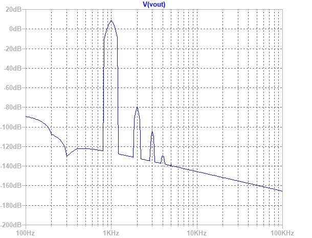
And if we increase power to about 12.5w into 8ohm, we still see a nice monotonically decreasing harmonic distortion profile. THD is now about 0.016%:
Comparing the 1 and 12 watt distortion profiles, the higher content of odd order distortion is already showing up in the 12 watt measurement.
But you can still consider it a nice distortion profile of a class A amplifier.
Now I am curious how the FFT profile looks when you measure at let's say 32 watt (16VRMS(45Vpk-pk)@8ohm).
I expect to see the typical class A/B distortion profile with higher odd order.
By the way wrt your post #1: this is not a SE amplifier.
Last edited:
41 watt class A/B amp with ~12 watts pure class A.
Daanve,
Where did you get this 12w value before this amp goes into Class AB - where is your simulation or did you build it and measure it? You make these statements to discredit this design, yet the proof in the simulation is quite obvious. I could even measure it with an O-scope and it will be the same. This amp is measuring very close to all predicted perfomance parameters and setpoints including quiscent bias current, 0v DC offset with no adjustments, 2.6mA LTP bias current, % thermal efficiency, clip point, etc...
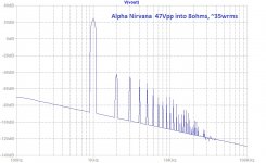
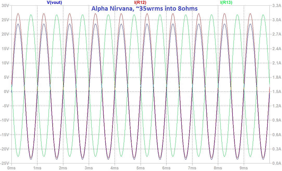
Here is the LTSpice sim running at 35w (well above 12w). The plot shows the usual output voltage as a function of time, plus the currents passing through the two Source resistors R12 and R13. The currents through these resistors is the same as the current passing through the MOSFETs. Note that the currents never dip below zero - the definition of Class A. As we can all see, the currents see-saw about the quiescent bias current of 1.7A, never dipping below zero, hence the MOSFETs never shut-off. True Class A operation until the stated clip level.
Schematic from Post 1 corresponding to this simulation:
Predicted source resistor currents on MOSFETs near clipping:
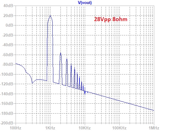
Here is the predicted FFT at 35wrms (47Vpp) into 8ohms. I haven't gotten around to making the FFT measurements yet:
Here are the distortion components and THD at 0.06% - not too bad. Still monotonically descending higher orders, lots of higher orders but odd orders are not higher than even orders as you predicted would happen on a Class AB-like topology:
Code:
Harmonic	Frequency	 Fourier 	Normalized	 Phase  	Normalized
 Number 	  [Hz]   	Component	 Component	[degree]	Phase [deg]
    1   	1.000e+03	2.362e+01	1.000e+00	   -0.88°	    0.00°
    2   	2.000e+03	1.079e-02	4.568e-04	 -135.36°	 -134.49°
    3   	3.000e+03	7.465e-03	3.160e-04	   64.66°	   65.53°
    4   	4.000e+03	4.712e-03	1.995e-04	    8.43°	    9.31°
    5   	5.000e+03	3.066e-03	1.298e-04	 -106.29°	 -105.41°
    6   	6.000e+03	1.394e-03	5.900e-05	 -178.14°	 -177.27°
    7   	7.000e+03	4.323e-04	1.830e-05	   61.48°	   62.36°
    8   	8.000e+03	2.457e-04	1.040e-05	  157.23°	  158.10°
    9   	9.000e+03	4.466e-04	1.891e-05	   84.64°	   85.52°
   10   	1.000e+04	4.541e-04	1.922e-05	  -15.46°	  -14.59°
   11   	1.100e+04	3.212e-04	1.360e-05	 -103.14°	 -102.27°
   12   	1.200e+04	1.729e-04	7.318e-06	  160.06°	  160.94°
   13   	1.300e+04	3.583e-05	1.517e-06	   70.99°	   71.86°
   14   	1.400e+04	4.479e-05	1.896e-06	  172.31°	  173.18°
   15   	1.500e+04	7.634e-05	3.232e-06	   72.65°	   73.53°
Total Harmonic Distortion: 0.060833%(0.060850%)
Attachments
Last edited:
Daanve,
Where did you get this 12w value before this amp goes into Class AB - where is your simulation or did you build it and measure it? You make these statements to discredit this design, yet the proof in the simulation is quite obvious.
The real class A output power (related to load impedance) can simply be calculated; how many examples do you want where this is clearly demonstrated? It is basic electronics (Elliott..Turner....Pass....Parker....).
With active components the maximum efficiency in class A is 25%; with inductive load the maximum is 50%.
I do not aim to discredit this design; I am confident it is quite good, and the distortion profile at almost full power looks OK (it is not a "specific" class A profile however as even quality class D amps improve on this), but:
1. It is not a class A amp up to full power;
2. It is not a SE amp.
I know that audio forums are fertile grounds for re-inventing the laws of physics, but I simply don't eat this....
Last edited:
“Not Class A” - Yet the currents in the MOSFETs never switch off up to full power.
Let’s move on.
Let’s move on.
Daanve,
Where did you get this 12w value before this amp goes into Class AB - where is your simulation or did you build it and measure it?
In case ... I'll do the math for you.
Output stage runs at 1.7 A (peak current).
Pk-pk current is 3.4 A.
This is 1.2 A RMS.
With an 8 ohm load the output stage delivers 8 x 1.2 = 9.6 VRMS in pure class A.
9.6 VRMS @ 8 ohm = 11.5 watt.
Agree?
Not for current source loaded output stages!
Doesn’t the SIT-3 use a similar topology in the output stage?
dave
Your math assumes a certain type of standard amp. Look at the LTspice sims - are they wrong?
Here, the current never drops below 150mA (axis on right). The sim is going to be more comprehensive than your back of the envelope calcs based on assumption of a certain type of amp. The CCS here is reactive (sort of like an inductor load would be) and there are bootstrap caps. Only the top MOSFET is driven by an audio signal from the VAS - hence SE Class A.
There are plenty of SE Class A amps in the Pass forum with 24v rails and 1.25A bias current that achieve 25w.
The simulation for the 35w case shows above where the current never switches off (Class A) is 47Vpp or 16.6Vrms. Power is V^2/R or 16.6^2/8=35w. So there’s my math.
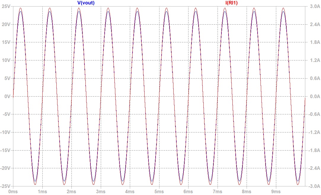
Your back of the envelope calcs neglect the fact that the reactive CCS produces a current that is 180deg out of phase with the top MOSFET, neither current ever dips below zero, but they combine out of phase to produce a peak current at the load that is about double the peak current in any one of the Source resistors - sort of like what happens on BTL amps. Here is the predicted current at the load resistor about 6App or or 2.12Arms, Power = I^2 x R or 2.12^2 x 8 = ~36wrms.
Here is the plot of the current at the load (RL1):
Using a rule of thumb for a certain generalized output topology can yield incorrect results. The LTSpice sim accounts for the actual topology used.
Here, the current never drops below 150mA (axis on right). The sim is going to be more comprehensive than your back of the envelope calcs based on assumption of a certain type of amp. The CCS here is reactive (sort of like an inductor load would be) and there are bootstrap caps. Only the top MOSFET is driven by an audio signal from the VAS - hence SE Class A.
There are plenty of SE Class A amps in the Pass forum with 24v rails and 1.25A bias current that achieve 25w.
The simulation for the 35w case shows above where the current never switches off (Class A) is 47Vpp or 16.6Vrms. Power is V^2/R or 16.6^2/8=35w. So there’s my math.
Your back of the envelope calcs neglect the fact that the reactive CCS produces a current that is 180deg out of phase with the top MOSFET, neither current ever dips below zero, but they combine out of phase to produce a peak current at the load that is about double the peak current in any one of the Source resistors - sort of like what happens on BTL amps. Here is the predicted current at the load resistor about 6App or or 2.12Arms, Power = I^2 x R or 2.12^2 x 8 = ~36wrms.
Here is the plot of the current at the load (RL1):
Using a rule of thumb for a certain generalized output topology can yield incorrect results. The LTSpice sim accounts for the actual topology used.
Attachments
Last edited:
This is almost exactly the same topology (differential input stage; CCS in the negative leg; comparable feedback):
20 Watt Class-A Amplifier
This design has +/- 22V rails and output stage current is 2.6A pk.
Amplifier is a little over 20 watt, class A.
Take notice of this quote:
Determining The Optimum Current
The ideal operating current for a Class-A amp will be about 110% of the peak speaker current. If the loudspeaker system has a nominal impedance of 8 Ohms (the design impedance for this amp), then with a +/- 22V supply the maximum (theoretical) speaker current is ...
I = V / R = 22 / 8 = 2.75A
In my original calculations, I decided on a quiescent current of 2.6A - this is really Ok, because the above calculation does not consider the losses in the output stage. In practice, it is likely that up to 3 Volts will be lost in the output circuit, based on the losses in the output devices, emitter resistors and driver transistors.
This now gives a maximum voltage of 19V peak (2.375A @ 8 Ohms). Applying the 110% fudge factor gives an operating current of 2.6125A, or 2.6A close enough. If these peaks are met in practice, this gives an output power of 22.5W into 8 Ohms.
Note that the current in the -ve supply rail remains constant, but that in the +ve supply rail will vary from the normal steady state current (same as the -ve supply). At signal extremes, the current will double (upper transistors turned on), or will drop to almost zero for negative peaks. This is common for single-ended Class-A amplifiers, although you will not see it stated in the text for most designs. This can complicate the design of the power supply.
Now I ask the acknowledged EE's here:
How can the Nirvana amp make 37 watts class A power with 1.7A pk current??
The 20 watt Elliott design complies with theory and practice: 2.6A pk current (+/- 22V rails) give 20 watt class A.
Is there a trick somewhere to have the Nirvana amp behave like one with ~3A pk current needed for 37 watt class A?
By the way: I stand corrected for the "not SE"; it is SE.
Last edited:
There are plenty of SE Class A amps in the Pass forum with 24v rails and 1.25A bias current that achieve 25w.
Aleph J comes closest in terms of topology (SE; CCS output stage).
It has +/- 24V rails and 2.5A pk, so output stage dissipation is 120 watts.
A little under 30 watt before clipping, so less than 25% efficient.
Again practice complies to theory.
What makes the Nirvana amp different??
Daanve,
Read very carefully Rod Eliot's comments on this topology:
This is precise way the Aleph J operates, and it is Class A amplifier in SEPP mode. The Nirvana extends its efficiency by careful drive of the output devices. Study it carefully; you will see it is achieved with bootstrap techniques.
There is no marketing sophistry, but clever topology, identified some years ago and championed by no less than Nelson Pass. In fact the peak current is not 1.7A, but 3.4A. I will not waste more words on explaining this to you further and leave it to you to figure out. So be it...... my thanks to X!
Hugh
Read very carefully Rod Eliot's comments on this topology:
In summary, the upper mosfet is direct driven from the earlier signal stages, giving it control of the voltage at the load at all times while the device is switched on. The lower pmos follows the upper device by see-sawing the currents through each device such that the sum of the two currents, Inmos and Ipmos, are conjugate - a sum of 3.4A at all times. In this way, the peak current through EACH device can be taken up to 3.4A from the quiescent 1.7A, whilst both devices are always on.The next step is to operate the current source at about 1/2 the speaker's peak current, and modulate its current output to ensure that both current source and power amplifier output device conduct during the entire signal cycle, but are able to vary their current in an appropriate manner. This improves efficiency (which remains dreadful, but slightly less so), and lowers the quiescent dissipation to more manageable levels.
The simple Class-A amplifier described by John L Linsley-Hood and the very similar looking Death of Zen (DoZ) amp on these pages use this latter approach, and it is a sensible variant of the various Class-A designs. As an example, the amplifier will only (?) need to dissipate about 50 Watts when idle, since the quiescent current is reduced to around 1.2 Amps.
Another version of the Class-A amp looks exactly the same as a standard Class-AB (Class-B) power amp, except the quiescent current is increased to just over 1/2 of the peak speaker current. This is thought by some that this is not a 'real' Class-A amplifier. It is real Class-A, and is best described as push-pull (as opposed to single ended) operation. If the bias current is not high enough for the actual reactive speaker load (not some quoted nominal resistive load), it is still possible that one transistor or the other will switch off at some part of the signal cycle. This will happen at a much higher power level than is normally the case, but if this happens, then the amplifier ceases to be true Class-A.
As an extension of the above, it is possible to design an amp that looks remarkably like a conventional Class-AB amp, but with additional circuitry is biased in such a way that the output transistors do not turn off - ever. This technique can also be used with Class-AB, and supposedly reduces crossover distortion.
This is precise way the Aleph J operates, and it is Class A amplifier in SEPP mode. The Nirvana extends its efficiency by careful drive of the output devices. Study it carefully; you will see it is achieved with bootstrap techniques.
There is no marketing sophistry, but clever topology, identified some years ago and championed by no less than Nelson Pass. In fact the peak current is not 1.7A, but 3.4A. I will not waste more words on explaining this to you further and leave it to you to figure out. So be it...... my thanks to X!
Hugh
Last edited:
The Aleph J runs on +/- 24V rails, +/- 2.5A pk-pk current (check manual).Daanve,
Read very carefully Rod Eliot's comments on this topology:
In summary, the upper mosfet is direct driven from the earlier signal stages, giving it control of the voltage at the load at all times while the device is switched on. The lower pmos follows the upper device by see-sawing the currents through each device such that the sum of the two currents, Inmos and Ipmos, are conjugate - a sum of 3.4A at all times. In this way, the peak current through EACH device can be taken up to 3.4A from the quiescent 1.7A, whilst both devices are always on.
This is precise way the Aleph J operates, and it is Class A amplifier in SEPP mode. The Nirvana extends its efficiency by careful drive of the output devices. Study it carefully; you will see it is achieved with bootstrap techniques.
Power dissipation of this amp is 200 watt; efficiency clearly less than 25%.
Bootstrapping might improve efficiency but not so much.
I can imagine you step out of the explanation 🙄I will not waste more words on explaining this to you further and leave it to you to figure out. So be it...... my thanks to X!
Hugh
Still curious after opinions of EE's.
Last edited:
Again quoting Elliott's comment on this topology:
Note that the current in the -ve supply rail remains constant, but that in the +ve supply rail will vary from the normal steady state current (same as the -ve supply). At signal extremes, the current will double (upper transistors turned on), or will drop to almost zero for negative peaks. This is common for single-ended Class-A amplifiers, although you will not see it stated in the text for most designs.
So, current swing is 5A pk-pk for Aleph J (conforms with class A output power).
I don't see much more than 3.4A pk-pk for Nirvana amp; maybe a bit more with bootstrapping, but 6A pk-pk??
Last edited:
- Home
- Amplifiers
- Solid State
- Discussion of Alpha Nirvana Operation