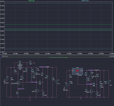
Seeing that -140dB line makes me happy 😀The higher voltage shouldn't be an issue. I'd have to test higher current configurations. I'll try to prepare a higher current testing setup.
This is just a sim but as a general example:
View attachment 1121362
It's at 36V/20A output. Seems it could be doable. I used some random high power MOSFET model just to see how it would behave.
Higher voltage should also work but at some point there's going to be heat buildup in certain parts of the circuit (clearly apart from the pass transistor). So might need to use lower current for the denoiser circuit, or upgrade the power rating of the BJTs.
edit: also in this configuration Q1 takes a big hit at startup with a high base current surge. A protection resistor will have to be added, output capacitance would have to be increased, C3's value lowered etc. It's just a general example only.
I wonder if something like this mosfet will work - IRFB3607PBF ?
Is it possible to use two, or say four of those for current sharing and to better spread the heat dissipation?
Is it possible to use two, or say four of those for current sharing and to better spread the heat dissipation?
That's N-channel, might work for negative output version. Positive needs P-channel.
I don't think I am equipped to test such output powers. I might try with a few amps output.
I don't think I am equipped to test such output powers. I might try with a few amps output.
Tried that IRFB3607PBF MOSFET for the negative voltage output version. 36V/100A output, seems to work with two in parallel. But I'm not sure about how large the source resistors should be. Input capacitors would need a 30mOhm total ESR, or lower if the source is lower than 10mOhm.
I might have made a mistake, never tried this before. No way of making a board for that kind of output current, I wouldn't be able to test it.
Different MOSFETs might improve performance a bit.
I attached a screenshot for +/- versions.
I might have made a mistake, never tried this before. No way of making a board for that kind of output current, I wouldn't be able to test it.
Different MOSFETs might improve performance a bit.
I attached a screenshot for +/- versions.
Attachments

Not sure if the source resistors are needed, but the voltage source needs a bit of output impedance, 10-20mOhms, and even lower input cap ESR.
Figured I'd update this thread as I designed a set of PCBs for the DC coupled denoiser.

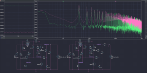
PCBs have RC/LC/FC input options, the LC version PSRR should be similar to this sim (with the parts I got):

Output impedance seems pretty good:

But having this on the PCB output is a bit of a challenge. I used 4mm wide traces, with 1 oz copper at around 4cm long traces their resistance comes out at ~5mOhm which is two orders of magnitude higher than the regulator output impedance (at 20kHz). So I cleared the solder mask and will try to solder 2mm diameter solid copper wire across the whole length of the traces. The wire should have around 200uOhm which is considerably lower.


Ordered the various SMD parts and I'll do a measurement session along with the LM3x7 boards from the Denoisator thread. Will update with measurements once I'm done.
PCBs have RC/LC/FC input options, the LC version PSRR should be similar to this sim (with the parts I got):
Output impedance seems pretty good:
But having this on the PCB output is a bit of a challenge. I used 4mm wide traces, with 1 oz copper at around 4cm long traces their resistance comes out at ~5mOhm which is two orders of magnitude higher than the regulator output impedance (at 20kHz). So I cleared the solder mask and will try to solder 2mm diameter solid copper wire across the whole length of the traces. The wire should have around 200uOhm which is considerably lower.
Ordered the various SMD parts and I'll do a measurement session along with the LM3x7 boards from the Denoisator thread. Will update with measurements once I'm done.
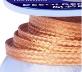
Copper braid should be simpler to stack. But solder has around 5 times higher resistance than copper, so ideally I'd use as much copper as possible. I'll play with both options.
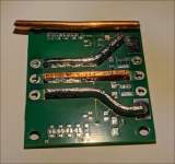
Tried it with the LM3x7 board (same 4mm wide output traces), I had to scrape off the solder mask as I didn't remove it for that design. Bit of a pain but worked out fine.
I used 6mm^2 section wire, I think it's between AWG 9 and 10, some 2.76mm diameter. The cable datasheet showed 3.08 Ohm per km which is a bit higher than pure copper (2.80 Ohm/km), so 1.1x multiplier compared to pure copper. So 4cm length should work out to about 123 uOhm.
I do have a thicker 10mm^2 section wire (unused piece in photos) which should work out at 74uOhm for 4cm. But not sure it fits. I'll have to also hammer it into a rectangular shape, maybe it fits.
edit: should I enlarge the output pads holes? they're 2mm atm
Attachments

Last edited:
Be careful: the deformation will cause strain-hardening and increase the resistivity unless you anneal it afterwards, thus it might be counter productiveI'll have to also hammer it into a rectangular shape, maybe it fits.
The solder wick should be simpler to work with but how much does it lower the resistance? Seems like a nice simple way to add some current carrying capability to smaller traces. But the extra solder doesn't do that much by comparison.
Interesting, I did not know that!Be careful: the deformation will cause strain-hardening and increase the resistivity unless you anneal it afterwards, thus it might be counter productive
Just been reading up on claude.ai tells me <2-3% though a lot depends on bend and not overworking it. Interesting stuff.
Yeah the 10mm^2 copper rod can be hammered to fit the 4mm wide trace. But just. Solder seems to wick underneath it on the trace, from first attempt experience, so using it should work out at ~80uOhm resistance, at 4cm length.
But I'm not sure it's worth the trouble since there should be low output impedance at PCB output, that's where I'm sensing with denoiser.
For DC 4mm wide tracks should already be enough. MOSFETs are some 8A rated (continuous) so they should be able to do 5A but limiting factor is heat in this case. Maybe 5A at 0.2Vdrop but input trace is just 1.5mm wide. I'd think 2A output should be fine for some 1W of dissipated heat? Output traces will work as heatsinks, and I also added some extra holes across them to help with air flow.
I'd keep solder mask off the +/-V output traces
I was trying to figure out if I can improve cooling even more and I remembered I have some small heatsink from my 3D printer stepper motor drivers. It does barely fit on top of the MOSFETs


But then I noticed their application on the driver PCB and figured I could do the same.


They moved the IC on the bottom of the PCB and used vias to transfer the heat on top of the PCB, where it goes into the heatsink. The heatsink has good surface for its small size.
The driver IC normally dissipates around 2.6W as per datasheet, but also has a high operating temperature rating, 125C.

Trying the same trick on my PCB design results in this:


I had to increase the board width by 3mm to have a more comfortable fit, so the board is 50mm x 53mm this way.
The heatsinks and the exposed output traces should allow for maybe 2W dissipated heat, comfortably. Hopefully.
But then I noticed their application on the driver PCB and figured I could do the same.
They moved the IC on the bottom of the PCB and used vias to transfer the heat on top of the PCB, where it goes into the heatsink. The heatsink has good surface for its small size.
The driver IC normally dissipates around 2.6W as per datasheet, but also has a high operating temperature rating, 125C.
Trying the same trick on my PCB design results in this:
I had to increase the board width by 3mm to have a more comfortable fit, so the board is 50mm x 53mm this way.
The heatsinks and the exposed output traces should allow for maybe 2W dissipated heat, comfortably. Hopefully.
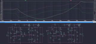
I'm trying to understand why the tempco of this latest incarnation of circuit looks way better than the AC-coupled denoiser version. And apart from other interactions, the fact that I modified the startup circuit seems to help.
Looking at the normal regulator without the denoising circuit, the new startup circuit seems to make for lower Vout variation due to temperature changes.

D3 can affect Vout while D1 doesn't do anything after startup.
It also isolates the two nets, and helps with PSRR

And this matters even more if we use the two Zeners back to back as Vref


There is a cost though, at least for the standard application there's one extra resistor that's being added to the circuit, and there's around 1mA flowing through that resistor chain, at all times. But for me it's totally worth the cost just for the better temperature variation performance. Let alone the boost in PSRR.
But even with the new startup circuit, there's still a lot of difference between the DC coupled and AC coupled denoising circuit. My best guess atm is that Vref tempco works against denoiser BJT tempco and they sort of cancel out.

edit:
For example in the DC-coupled versions using a blue LED as Vref has tighter Vout across temperature than using the two Zeners back to back which makes me think that LED tempco works against BJT tempco. And if it works like this in practice, that would make the blue LED the superior Vref for the DC-coupled circuit.

And there doesn't seem to be any difference between PSRR performance in both LED or Zener back to back cases. If anything the Zeners need a bit more current.

The simulations are for both 25C and 75C, so 50C span between same colored traces.
Looking at the normal regulator without the denoising circuit, the new startup circuit seems to make for lower Vout variation due to temperature changes.
D3 can affect Vout while D1 doesn't do anything after startup.
It also isolates the two nets, and helps with PSRR
And this matters even more if we use the two Zeners back to back as Vref
There is a cost though, at least for the standard application there's one extra resistor that's being added to the circuit, and there's around 1mA flowing through that resistor chain, at all times. But for me it's totally worth the cost just for the better temperature variation performance. Let alone the boost in PSRR.
But even with the new startup circuit, there's still a lot of difference between the DC coupled and AC coupled denoising circuit. My best guess atm is that Vref tempco works against denoiser BJT tempco and they sort of cancel out.
edit:
For example in the DC-coupled versions using a blue LED as Vref has tighter Vout across temperature than using the two Zeners back to back which makes me think that LED tempco works against BJT tempco. And if it works like this in practice, that would make the blue LED the superior Vref for the DC-coupled circuit.
And there doesn't seem to be any difference between PSRR performance in both LED or Zener back to back cases. If anything the Zeners need a bit more current.
The simulations are for both 25C and 75C, so 50C span between same colored traces.
Last edited:
Also the Vref LED needs at least one Vbe extra Vdrop on top of CCS LED. I suppose a IR CCS LED + a red LED as Vref would also be possible (if you absolutely hate the resulting magenta light).
Last edited:
I have successfully used the LED of a peculiar optocoupler (6N139) as a Vbe compensation:
This opto uses a visible LED, unlike regular ones, and works nicely to compensate the Vbe (that's reality: sim might be different)
Those simple discrete regulators come basically in two flavors: one is the follower output, as shown by Patrick, the other is the common-emitter output.
Both have their peculiarities and advantages: the common-collector is self-starting and more familiar, but the C.E. is LDO by nature, and it has the potential to provide better performances, since the reference voltage will generally be created from the output.
This however makes it non-self-starting. This can be seen as a liability but also as an advantage.
I generally manage to make an advantage of it, like in this example:
A PSU...
- Home
- Amplifiers
- Power Supplies
- Discrete regulators with denoiser