Try to test 5-th circuit on WEB link below (english).
Circuit (pre-tracking regulator) works very good.
We tested this PSU circuit for HI-END low noise pre amplifier (low noise line pre amplifier for bobbin tape recorder).
LED in circuit is 2.8 - 3 Volts across.
.
Using 3-pin regulators off-piste: part 4
.
Circuit (pre-tracking regulator) works very good.
We tested this PSU circuit for HI-END low noise pre amplifier (low noise line pre amplifier for bobbin tape recorder).
LED in circuit is 2.8 - 3 Volts across.
.
Using 3-pin regulators off-piste: part 4
.
Last edited:
I remember measuring 150+dB of PSRR from this version of supply (positive output). I think it was around 155, and simulation says it should be 160.
But my 60dB LNA and ADC combo are not enough to accurately measure 160dB PSRR. I'm currently working to make a fresh pcb for that ADC chip, so I have less LF noise, which would allow me to measure the PSRR better.
Right now I did a ballpark calibration for the ADC+LNA combo, and noisefloor of the supply + LNA seems to be around the 800-900pV/sqrtHz level.
My LNA should be around 450pV/√Hz, which would put the supply's noisefloor at around 660-780pV/√Hz.
I didn't yet measure the output impedance, but simulation says it should be very low.
This supply already has way more performance than it's needed in this application. I also have a cap multi in front of the DAC board. So in total I have over 200dB of PSRR, which is really stupid high in this case.
This board is more of an application for this circuit, so I see how it behaves in the real world. And the capacitance multiplier is mostly there to drop some voltage so I can get away without using heatsinks on the pass transistors.
All in all even if this is a nice supply, I recommend using a LM317 + denoiser in this type of application. Simpler to implement and less chances of instabilities. DAC output noise will dominate anyway.
I personally have no reason to try other circuits, especially at this point. Maybe on other projects.
Attachments
I don't mind it, but I did change the theme maybe it's more clear now? I also put the window fullscreen for more detail.
I prefer dark themes while working on the PC at night.
I prefer dark themes while working on the PC at night.
Attachments
Last edited:
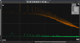
Made a new set of measurements for the CCS loaded version of the negative feedback supply (with MOSFET as pass transistor).
If we remove the 10R protection resistor then we can really get the noise down.
I tested both positive and negative output versions. You can use the same pcb (will upload updated design in following post) for both positive and negative output, just rotate all polarized parts and swap transistors for their complementary with the following exceptions:
- for pass transistor you can use whatever you want, within reason. I chose the cheapest TO220 ones I could fine and seem to work fine. I made some sim tests with different models I found and seemed to work fine with all, with minor differences.
You could use say a SOIC-8 transistor which allows for a max of 2.5W TDP, so might fit the bill for some 100mAout max circuit.
Also BJTs seem to work here.
- for negative output version the BJT driving the gate of the pass transistor should be 2N5401.
The pcb was set up with 18Vin with 200uF after the rectifying bridge and 12Vout with 150R load making for a total of around 100mA out and the input ripple situated at around 0dBV.
Output capacitor was Panasonic FR 470uF/25V (EEUFR1E471L) for both positive and negative output versions.
Compensation values were 33nF/1R on all tests with some exceptions:
- if you want to use the ZTX pair for the denoising circuit then you need to install some 20nH in series with the output cap, else it's not stable. Having a ZTXx81 transistor in the dienoiser position (both positive and negative) requires that extra inductor for stability. Having a MPSAx6 in that position does not require the extra inductor.
- I could get the CCS loaded denoiser version (with ZTX851 on positive output version) stable without any compensation network, and also this is the lowest noise version (same with negative output version) at around 230pV/sqrtHz level. The negative output version wasn't stable in this configuration (ZTX951) without the compensation network.
Further testing is required for example with the ferrite bead mentioned here by jackinnj. The BJT footprint should allow for a berrite bead on its leg.
Max PSRR for the negative output version was around 140dB. There wasn't much difference between dienoiser and denoiser configurations. The dienoiser brings 5-7dB of total PSRR while increasing the noise (over denoiser).
Lowest noise was with CCS loaded denoiser with ZTX951 at around 230pV/sqrtHz level (without LNA's noise).
Max PSRR for the positive output version is a bit tricky. I could get it between 163dB and 171dB depending on how I oriented the DUT on my desk. This was for the MPSAx6 pair.
ZTX pair has a PSRR of around 140dB.
ZTX851+MPSA56 - 141dB
ZTX951+MPSA06 - 157dB
MPSAx6 pair - 171dB
Lowest noise was with CCS loaded denoiser with ZTX851 at the same 230pV/sqrtHz (without LNA's noise) as the negative version. PSRR for this setup is around 130dB.
The measurements I attached contain some of the measurements at higher CCS current. I recommend using 100R for around 10mA, but lowest noise/PSRR I got by pushing it to around 17mA with 60R.
Didn't seem stable with 50R, so I'd say 60R minimum (for max current), 100R recommended.
The boards I measured were both fitted with the LEDs Vref version.
Attachments
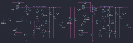
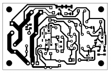
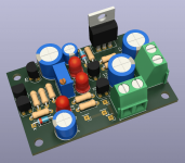
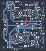
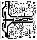
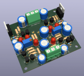
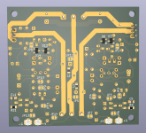
I updated the pcb design for the negative feedback version, single and dual versions.
Both designs are DIY-able. The single has two top-side passes, the dual has three. Gerbers have them included.
Schematic and pcb PDF files are inside the zip file, as well as the Kicad projects and gerber files.
There's jumpers allowing for any configuration. For example if you don't like the LEDs you can use BZX84Cxx Zener diodes (SOT-23 footprints), or LM329 and omit the CCS transistor.
BJT footprints are for MPSAx6. Using other types might require you to rotate or adapt the transistors to the existing footprints.
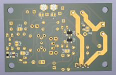
I completely dropped the rectifying part of the PCB. That should happen further away from the low noise outputs of the supply. This way the boards got smaller.
Single pcb is 57mm x 37mm and dual pcb is 61mm x 67mm.
Power traces are exposed so you can fill them with solder to decrease their resistance.
As with all my designs they are free for personal use, no commercial applications.
edit: Measurements were done on the previous single pcb version. The updated version misses the rectifying part and has some extra jumpers.
The dual board is not tested so you make it at your own risk.
Both designs are DIY-able. The single has two top-side passes, the dual has three. Gerbers have them included.
Schematic and pcb PDF files are inside the zip file, as well as the Kicad projects and gerber files.
There's jumpers allowing for any configuration. For example if you don't like the LEDs you can use BZX84Cxx Zener diodes (SOT-23 footprints), or LM329 and omit the CCS transistor.
BJT footprints are for MPSAx6. Using other types might require you to rotate or adapt the transistors to the existing footprints.
I completely dropped the rectifying part of the PCB. That should happen further away from the low noise outputs of the supply. This way the boards got smaller.
Single pcb is 57mm x 37mm and dual pcb is 61mm x 67mm.
Power traces are exposed so you can fill them with solder to decrease their resistance.
As with all my designs they are free for personal use, no commercial applications.
edit: Measurements were done on the previous single pcb version. The updated version misses the rectifying part and has some extra jumpers.
The dual board is not tested so you make it at your own risk.
Attachments
-
 Screenshot_20220220_140918.png20.2 KB · Views: 248
 -
 Screenshot_20220220_141158.png13.3 KB · Views: 267
 -
 Screenshot_20220220_135918.png107.3 KB · Views: 267
 -
 Screenshot_20220220_141036.png126.9 KB · Views: 265
 -
 Screenshot_20220220_131308.png27.5 KB · Views: 240
 -
 Screenshot_20220220_132120.png22.4 KB · Views: 254
 -
 Screenshot_20220220_131618.png147.9 KB · Views: 249
 -
 Screenshot_20220220_131830.png162.9 KB · Views: 264
 -
pcb.zip1.2 MB · Views: 155

Surely you are not, it's a mixed bag and depends from person to person. This is personal preference and depends largely on the environment.
Say in a business setup at the office, yeah, maybe it's more useful for anyone involved to see the same thing.
For me, I got darktheme setting on for the forum, and at night the contrast looks better for my eyes.
But if you download the sim file you can enjoy your color scheme you have set in your LTSpice.
The theme is not easily switchable so I'll post them like this.
There is no right answer without further context, regarding the color theme in LTSpice.
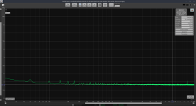
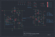
I've made a 5Vout version of the supply, and measured it. With such low voltage output there are a few considerations.

First of all the coupling capacitor (C3/C11) on the output of the denoising circuit needs to be flipped on the PCB.
The resistor from the starting circuit (R2/R16) needs to be around 33k for the minimum 7Vin. Don't go higher for this value or the regulator doesn't start.
C2/C10 recovers some of the PSRR performance that is lost by adding R2/R16, but this value can't be too high. A max of 22uF seems ok. With higher values we get a voltage spike on the output, at startup.
I suppose a good solution would be to disconnect R2/R16 after the supply settles a bit, with a relay maybe? This way we can get a bit more PSRR performance at lower frequencies. But 22uF seems to be a good compromise.
With such low Vout I couldn't use anything else other than two LEDs for Vref. Tempco might not be great but it's not horrible either. I didn't test this, just going by simulation results.
I measured using the values in the above schematic, for both denoiser and dienoiser configuration, with both ZTX851 and MPSA06 in the denoiser BJT spot.
For denoiser with just ZTX851 R17 should be 39k-43k, for MPSA06 it should be 56k-62k.
R9 was 220k for any of the two BJTs in dienoiser configuration.
I made PSRR measurements at 105Hz, 440Hz, 1kHz, 5kHz and 15kHz, using a ripple injector powered by batteries. LNA also powered by batteries.
Measurements are pretty close to what the simulation predicts, apart from the voltage on the positive side of C3/C11, which was closer to around 3-3.5VDC.
Input voltage was around 10-11V with around 0.5Vrms ripple. Out measurements were made right at the output connector. I used 50R load for 100mAout for all measurements.
I attached all measurements in a zip file but in this list I extracted the PSRR and noise values for just the DUT.
denoiser configuration:
- MPSA06:
105Hz: 124.5dB
440Hz: 138.2dB
1kHz: 131.3dB
5kHz: 111.8dB
15kHz: 93.6dB
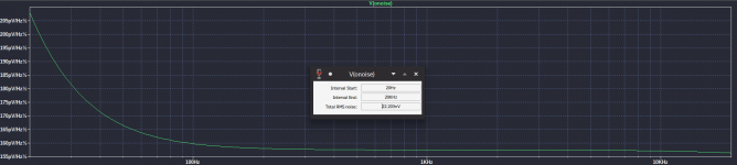
noise: 61nV | ~436pV/sqrtHz
- ZTX851:
105Hz: 125dB
440Hz: 139.6dB
1kHz: 132.4dB
5kHz: 112.8dB
15kHz: 94.5dB
noise: 34.3nV | ~222pV/sqrtHz
dienoiser configuration:
- MPSAx6:
105Hz: 146.8dB
440Hz: 147.3dB
1kHz: 143.9dB
5kHz: 137.5dB
15kHz: 117.9dB
noise: 77nV | ~540pV/sqrtHz
- MPSA56_ZTX851:
105Hz: 143.3dB
440Hz: 148.3dB
1kHz: 145.8dB
5kHz: 140.6dB
15kHz: 116.2dB
noise: 61nV | ~436pV/sqrtHz
grounded lna noise: 61.8nV | ~427pV/sqrtHz
Noise in nV is for 20Hz-20kHz. Noise in pV/sqrtHz is valid for most audio spectrum, at LF might be a bit higher level.
I also included a noise measurement for a 33R resistor (33R resistor noise + LNA noise) as a sanity check, because the ZTX851 denoiser noise is so low that I had to make sure. I think in that configuration the regulator noise is equivalent to the thermal noise of a 3.5R resistor, which is very low. I'm not even sure if such low noise is needed for anything in audio. In that configuration PSRR at 100Hz is not that bad, about 125dB. Could get higher if the startup resistor is removed from the circuit after startup, but I didn't measure this.
I also didn't build/measure the negative version of this setup, but I included both negative versions in the attached LTSpice sim file. Q12/Q17 from the sim file should be 2N5401 for the negative versions.
Noise measurements in the attached zip file include LNA's noise.
Ah yes, almost forgot: after startup first swing goes to 5.5-5.6V, then settles at 5V in half a minute or so. So if you want to use this first check that your circuit can deal with the first higher swing.
First of all the coupling capacitor (C3/C11) on the output of the denoising circuit needs to be flipped on the PCB.
The resistor from the starting circuit (R2/R16) needs to be around 33k for the minimum 7Vin. Don't go higher for this value or the regulator doesn't start.
C2/C10 recovers some of the PSRR performance that is lost by adding R2/R16, but this value can't be too high. A max of 22uF seems ok. With higher values we get a voltage spike on the output, at startup.
I suppose a good solution would be to disconnect R2/R16 after the supply settles a bit, with a relay maybe? This way we can get a bit more PSRR performance at lower frequencies. But 22uF seems to be a good compromise.
With such low Vout I couldn't use anything else other than two LEDs for Vref. Tempco might not be great but it's not horrible either. I didn't test this, just going by simulation results.
I measured using the values in the above schematic, for both denoiser and dienoiser configuration, with both ZTX851 and MPSA06 in the denoiser BJT spot.
For denoiser with just ZTX851 R17 should be 39k-43k, for MPSA06 it should be 56k-62k.
R9 was 220k for any of the two BJTs in dienoiser configuration.
I made PSRR measurements at 105Hz, 440Hz, 1kHz, 5kHz and 15kHz, using a ripple injector powered by batteries. LNA also powered by batteries.
Measurements are pretty close to what the simulation predicts, apart from the voltage on the positive side of C3/C11, which was closer to around 3-3.5VDC.
Input voltage was around 10-11V with around 0.5Vrms ripple. Out measurements were made right at the output connector. I used 50R load for 100mAout for all measurements.
I attached all measurements in a zip file but in this list I extracted the PSRR and noise values for just the DUT.
denoiser configuration:
- MPSA06:
105Hz: 124.5dB
440Hz: 138.2dB
1kHz: 131.3dB
5kHz: 111.8dB
15kHz: 93.6dB
noise: 61nV | ~436pV/sqrtHz
- ZTX851:
105Hz: 125dB
440Hz: 139.6dB
1kHz: 132.4dB
5kHz: 112.8dB
15kHz: 94.5dB
noise: 34.3nV | ~222pV/sqrtHz
dienoiser configuration:
- MPSAx6:
105Hz: 146.8dB
440Hz: 147.3dB
1kHz: 143.9dB
5kHz: 137.5dB
15kHz: 117.9dB
noise: 77nV | ~540pV/sqrtHz
- MPSA56_ZTX851:
105Hz: 143.3dB
440Hz: 148.3dB
1kHz: 145.8dB
5kHz: 140.6dB
15kHz: 116.2dB
noise: 61nV | ~436pV/sqrtHz
grounded lna noise: 61.8nV | ~427pV/sqrtHz
Noise in nV is for 20Hz-20kHz. Noise in pV/sqrtHz is valid for most audio spectrum, at LF might be a bit higher level.
I also included a noise measurement for a 33R resistor (33R resistor noise + LNA noise) as a sanity check, because the ZTX851 denoiser noise is so low that I had to make sure. I think in that configuration the regulator noise is equivalent to the thermal noise of a 3.5R resistor, which is very low. I'm not even sure if such low noise is needed for anything in audio. In that configuration PSRR at 100Hz is not that bad, about 125dB. Could get higher if the startup resistor is removed from the circuit after startup, but I didn't measure this.
I also didn't build/measure the negative version of this setup, but I included both negative versions in the attached LTSpice sim file. Q12/Q17 from the sim file should be 2N5401 for the negative versions.
Noise measurements in the attached zip file include LNA's noise.
Ah yes, almost forgot: after startup first swing goes to 5.5-5.6V, then settles at 5V in half a minute or so. So if you want to use this first check that your circuit can deal with the first higher swing.
Attachments
I also made a small update to the PCB designs. The potentiometer is now in parallel with the lower resistor, so you install one or the other. It was between the two resistors in previous designs.
C4 polarity is correct for 12Vout and up. For 5Vout you need to flip its polarity. If you want to build the board for any Vout it's best you ask here if anything is not clear.
Zip files contain the Kicad design files, schematics PDF files, board DIY print files and gerber files. I release the designs only for personal use, no commercial uses.
Attachments
Minimum Vdrop across the regulator seems to be around 0.33V (with IRF9520) to still keep good performance. There is a bit of degrading compared to 3-4Vdrop but doesn't seem to affect the 100Hz area much.
I have not tested this, I'm just going by simulation results:

I have not tested this, I'm just going by simulation results:
Attachments
I managed to find a way to simulate PSRR without the startup resistor in circuit:

This way I don't have to bypass D4 with a capacitor and get that nasty startup spike.
I am not sure of the final implementation for removing that resistor, I just like how performance looks without it.
The 1n4148 bypass diodes bring the startup swing to a low level:

I used a random pass mosfet in the sim file, something that has a similar response to what I want to use (IRF9520), and I put R10 to tame the 1MHz peak but might not be necessary for IRF9520.
This way I don't have to bypass D4 with a capacitor and get that nasty startup spike.
I am not sure of the final implementation for removing that resistor, I just like how performance looks without it.
The 1n4148 bypass diodes bring the startup swing to a low level:
I used a random pass mosfet in the sim file, something that has a similar response to what I want to use (IRF9520), and I put R10 to tame the 1MHz peak but might not be necessary for IRF9520.
Attachments
How much is the max output current of above circuit? If I have the electronic kit that required voltage 5 VDC and 4 Amps, can I use the circuit? any modification required?Minimum Vdrop across the regulator seems to be around 0.33V (with IRF9520) to still keep good performance. There is a bit of degrading compared to 3-4Vdrop but doesn't seem to affect the 100Hz area much.
I have not tested this, I'm just going by simulation results:
View attachment 1071992
All current goes through MOSFET. M2 So pick a powerful one, cool it for a wattage Vdrop X currentHow much is the max output current of above circuit? If I have the electronic kit that required voltage 5 VDC and 4 Amps, can I use the circuit? any modification required?
I only played with around 1Aout max I think. It should work, maybe a beefier MOSFET. I will revisit this at some point and do some higher power measurements.How much is the max output current of above circuit? If I have the electronic kit that required voltage 5 VDC and 4 Amps, can I use the circuit? any modification required?
Here's an example for 5V/4A output. With 5Vout Vref has to be two series LEDs so tempco is not going to be great. There's 0.25V variation 25-70 degrees C. But else it seems like it should work. I need to test this but I don't think I have the higher power IRF9530. I'll look and see if I can find something similar, or use a bit lower current with IRF9520.How much is the max output current of above circuit? If I have the electronic kit that required voltage 5 VDC and 4 Amps, can I use the circuit? any modification required?
PSRR is decent, noisefloor is very low.
I used 8Vin but I might be able to get it lower. Don't think you'll have this performance with way less.
Attachments

They look amazing!I updated the pcb design for the negative feedback version, single and dual versions.
Both designs are DIY-able. The single has two top-side passes, the dual has three. Gerbers have them included.
Schematic and pcb PDF files are inside the zip file, as well as the Kicad projects and gerber files.
There's jumpers allowing for any configuration. For example if you don't like the LEDs you can use BZX84Cxx Zener diodes (SOT-23 footprints), or LM329 and omit the CCS transistor.
BJT footprints are for MPSAx6. Using other types might require you to rotate or adapt the transistors to the existing footprints.
I completely dropped the rectifying part of the PCB. That should happen further away from the low noise outputs of the supply. This way the boards got smaller.
Single pcb is 57mm x 37mm and dual pcb is 61mm x 67mm.
Power traces are exposed so you can fill them with solder to decrease their resistance.
As with all my designs they are free for personal use, no commercial applications.
edit: Measurements were done on the previous single pcb version. The updated version misses the rectifying part and has some extra jumpers.
The dual board is not tested so you make it at your own risk.
I am assuming these are more suited for low current applications?
I wonder what it will take to convert these to obnoxious levels of voltage and current of say 36V and 18A to 20A? Or maybe 34V 18A?
Reason is - it would be nice to have such regulated psu for Modulus 286 amp that used two LM3886 in parallel.
I wonder what it will take to convert these to obnoxious levels of voltage and current of say 36V and 18A to 20A? Or maybe 34V 18A?
Reason is - it would be nice to have such regulated psu for Modulus 286 amp that used two LM3886 in parallel.
The higher voltage shouldn't be an issue. I'd have to test higher current configurations. I'll try to prepare a higher current testing setup.
This is just a sim but as a general example:

It's at 36V/20A output. Seems it could be doable. I used some random high power MOSFET model just to see how it would behave.
Higher voltage should also work but at some point there's going to be heat buildup in certain parts of the circuit (clearly apart from the pass transistor). So might need to use lower current for the denoiser circuit, or upgrade the power rating of the BJTs.
edit: also in this configuration Q1 takes a big hit at startup with a high base current surge. A protection resistor will have to be added, output capacitance would have to be increased, C3's value lowered etc. It's just a general example only.
This is just a sim but as a general example:
It's at 36V/20A output. Seems it could be doable. I used some random high power MOSFET model just to see how it would behave.
Higher voltage should also work but at some point there's going to be heat buildup in certain parts of the circuit (clearly apart from the pass transistor). So might need to use lower current for the denoiser circuit, or upgrade the power rating of the BJTs.
edit: also in this configuration Q1 takes a big hit at startup with a high base current surge. A protection resistor will have to be added, output capacitance would have to be increased, C3's value lowered etc. It's just a general example only.
Attachments
Last edited:
- Home
- Amplifiers
- Power Supplies
- Discrete regulators with denoiser