Are you sure that there Are enought current from Q7 to PM829 circuit? Walt j uses about 8mA?
Thanks again.
It seems that past 5mA the tempco gets very good. The issue with the BJT pass transistor versions is that this current is not constant with a varying load. Hence the GLED block helps keep a constant current through the PM829 circuit.
Once there's 6mA or so through it the GLED doesn't help with tempco, but it does help with keeping a steady current through the diodes.
This is not the case for the MOSFET version as the current variation is low.
In the attached photo, you set the min current through the PM829 circuit with R2. That sets the minimum current when the regulator is under load. When there's no load, there's extra current flowing through the PM829 circuit, which would get shunted by the GLED transistor.
In the second circuit you set the min current with R20 (also valid for the MOSFET version of this circuit).
Attachments

Okay great job.
I think you can use R8 =80ohm for the BJT/ PM829 circuit from post #11. (12V output )
You have writtin 60-220 in the circuit.
We must see when the circuit have been built.
Cool.
I think you can use R8 =80ohm for the BJT/ PM829 circuit from post #11. (12V output )
You have writtin 60-220 in the circuit.
We must see when the circuit have been built.
Cool.
I will try testing the PM829 setup later today. I can use the hot air station to heat the area from some distance, and keep a thermometer to read the temp of the diodes, while checking the output voltage.
Also I need to check the noise of this setup. The noise of a single Zener didn't look that great, as profile, vs LED with the denoiser setup (which should have the lowest noise vs dienoiser).
Also I need to check the noise of this setup. The noise of a single Zener didn't look that great, as profile, vs LED with the denoiser setup (which should have the lowest noise vs dienoiser).
Boards
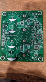
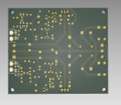
My boards arrived from JLCPCB, looking pretty good for the cheap option. I am going to check to make sure I am not missing anything and get to building it. This is from the Gerber's at post#11
If there has been a BOM correction or change can you let me know, I will read through the entire thread again but it's easy to miss things.
Cheers
Attachments
This is the discrete regulator with denoiser thread, not LM3x7. I am also not "sadface" who designed those boards. That pcb is not designed by me.
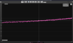
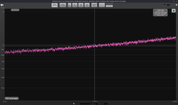
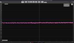
I measured the noise of the MOSFET version of the circuit with the GLED setup using a single 6.2V Zener, two LEDs in series and also the PM829 setup using two 6.2V Zeners.
Indeed the PM829 had the least drift. The LEDs have negative tempco, and they also seem to be more impervious to small currents of hot air.
Both the single Zener and PM829 have a worse noise and noise profile between 10kHz-20kHz vs the LEDs, in denoiser setup. The PM829 setup showed 100pV/sqrtHz all around higher noise than the single Zener version.
The dienoiser noise performance is identical between all setups.
So if you're looking for the lowest possible noise, use a single ZTX851 for the denoiser circuit, with the GLED setup. Tempco is not bad for general analog audio stuff.
If you're looking for good tempco and low noise then use PM829 with dienoiser with ZTX851/ZTX951. It will have slightly higher noise than denoiser.
Attached photos:
1. Single Zener noise with denoiser.
2. PM829 noise with denoiser.
3. PM829 noise with dienoiser.
4. GLED (two red LEDs) noise with dienoiser.
The dienoiser was used with ZTX851/MPSA56. Shorted LNA shows around 495pV/sqrtHz so you'd have to subtract it from the measured values in the photos for the real noise of just the DUT.
edit: you can check the denoiser noise with the LEDs and ZTX851 in post #94
Attachments

Well b*llocks, right thread wrong boards. I need to name my files better. I will order the correct boards as my next trick.
QUOTE=Trileru;6602353]This is the discrete regulator with denoiser thread, not LM3x7. I am also not "sadface" who designed those boards. That pcb is not designed by me.[/QUOTE]
QUOTE=Trileru;6602353]This is the discrete regulator with denoiser thread, not LM3x7. I am also not "sadface" who designed those boards. That pcb is not designed by me.[/QUOTE]
This is the discrete regulator with denoiser thread, not LM3x7. I am also not "sadface" who designed those boards. That pcb is not designed by me.
I’m still waiting for your discrete +-15-24v supply though 🙂
You can use a 20K pot instead of R24/R25. If Vref is around half of the output voltage the two resistors would have a similar value.
OK, it works. Some values however, according to simulation at least, lead to oscillation. In some short range the difference in voltage is what i need for now so its fine I ll use a pot only for R24.
I also had to increase the output resistors. Are these needed, or are the loads simulated? I had to increase values to reduce below dissipation below 5W. Of course if these are the loads then 20-25W is fine for a LTP/VAS.
Since this is for audio, I should look for values at 10Hz-100KHz, or broader range matters?
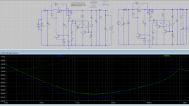
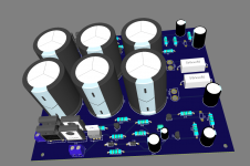
BTW it gives excellent measures at simulation and already created a 1st version of the PCB with both negative and positive, I attach a 3D photo
Attachments
The output resistors are the loads. What output current do you need? The input capacitance seems way too much.
Also with just the Zener you won't have a great tempco. And I can't really tell your part values from the picture.
Also with just the Zener you won't have a great tempco. And I can't really tell your part values from the picture.
The input capacitance is big because I have to give the CLC filter proper values to have the pole below 10Hz. But everything seems OK now, I am uploading the file, you will do better work than me. 🙂
The load I am expecting is 1-2mA for LTP and 50-100 mA for VAS. They have both voltages assigned. So V+- should be around 80V
I would like to keep the CLC filter. It gave such great results on my other project - A pure 200W Class A amplifier.
The load I am expecting is 1-2mA for LTP and 50-100 mA for VAS. They have both voltages assigned. So V+- should be around 80V
I would like to keep the CLC filter. It gave such great results on my other project - A pure 200W Class A amplifier.
Attachments
I think that's totally overkill. The noisefloor of the regulator should be around -180dBV mark, so pushing the ripple way under it doesn't help with anything. Also if you suspect you'd have HF noise that has to be attenuated this much you should probably fix those issues first.
You'd have more stray pickup by the copper traces anyway. I'd avoid using ground planes or wide traces.
You'd have more stray pickup by the copper traces anyway. I'd avoid using ground planes or wide traces.
OK, will try both ways when I put this in reality and decide. BTW now I realized what PM829 is.... I just included it.
Here's what a 1uH/470uF LC filter does to the overall PSRR. The first cap in CLC sets the input ripple into the regulator, I'd use something like 470uF for it as well. For 100mAout it should be fine.
edit: you need the LC filter to work in the HF zone where the regulator's PSRR is not so great. No need to make it active at lower frequencies.
Also try choosing an inductor that has some resistance. I used 100mOhm in the sim for it.
edit: you need the LC filter to work in the HF zone where the regulator's PSRR is not so great. No need to make it active at lower frequencies.
Also try choosing an inductor that has some resistance. I used 100mOhm in the sim for it.
Attachments
Last edited:
Where are you sensing the noise for the denoiser? At the output of the pcb or are you sensing at the load?
The performance of the circuit is highly dependent on the pcb layout. I can only guarantee the performance on the design I made and measured.
The performance of the circuit is highly dependent on the pcb layout. I can only guarantee the performance on the design I made and measured.
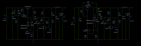
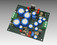
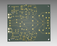
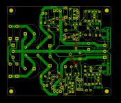
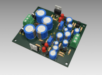
Made a dual pcb for the positive feedback version. It should be good for around 100-200mAout.
There's an input CRC/CLC filter, 16mm diameter capacitor footprints. You can install the PM829 setup instead of the LEDs, just install the diodes vertically.
The board can be diyed, and the size is about 87mm x 75mm. You'd need to install a total of 4 topside links if diy (red traces).
I'll make a dual version for the other circuit, maybe for the high power output MOSFET version as well.
This design has not been tested so you make it at your own risk! I did follow the general rules I did when I made the single versions so it should perform similarly.
It can also be used with either a center tapped transformer either with a single secondary one.
edit: cleaned schematic and set the correct BJT footprints. for certain output voltages it's better to ask here than follow the schematic part values.
Attachments
Last edited:
Where are you sensing the noise for the denoiser? At the output of the pcb or are you sensing at the load?
The performance of the circuit is highly dependent on the pcb layout. I can only guarantee the performance on the design I made and measured.
You mean on the simulation? At the output of the pcb.
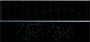
This is the negative feedback version dual pcb. Same deal as the other one, just that it has only 3 topside links. Can also be diyed.
Hope I have the time to make the MOSFET dual version for this circuit.
Hope I have the time to make the MOSFET dual version for this circuit.
Attachments

- Home
- Amplifiers
- Power Supplies
- Discrete regulators with denoiser