Where do you get the idea that there is asymmetry in the Toshiba 2SK170, 2SJ74 jfets? Are you confusing these with American jfets?
I thought I saw conversation in your blowtorch thread and perhaps Patrick may have mentioned it. not that they arent symmetrical, just that there was one or 2 parameters that wasnt exactly the same when reversed, but I cant find it again now. it IS possible i'm confusing it with another part, I actually hope I am
Last edited:
I am pretty sure that, for all practical purposes, both the Toshiba N and P jfets are symmetrical and will work 'upside-down' just as well.
This has NOTHING with trying to make an N into P or anything like that, as N and P jfets have opposite 'doped' channel material, so they are forever different.
This has NOTHING with trying to make an N into P or anything like that, as N and P jfets have opposite 'doped' channel material, so they are forever different.
The American N channel jfet the J113 is NOT completely symmetrical. This is important sometimes, but not too often. This is due to the wafer fabrication. The pin outs are really different and cause problems.
The so called "short channel" JFETs you can reverse the Source and Drain and the device dosen't not know the difference. It's not that an N becomes a P. Just that you can switch the source and drain. I honestly don't remeber the structure enough to explain more. All JFETs do not have the same physical structure or channel length and gate layout? Wish I was so interested when I was working in an area I could learn all this. Now I just work with multi phase switching stuff for processor and memory server board applications. Certanly I'ld rather work in an audio function somehow but that's all filtered down to Class D or ? Mid-Fi analog Yuk 😱
'using as' P channel (acting as, not changing the atomic structure, didnt I make this correction already?)This has NOTHING with trying to make an N into P or anything like that, as N and P jfets have opposite 'doped' channel material, so they are forever different.
re J113: hmm no I dont think thats the fet, i'm going to have to do some more searching to see where this was discussed, one of the many threads lamenting the lack of P-channels
No way. JFETs are symmetrical, mostly, for an interchange of the leads labeled "source" and "drain", but that doesn't make them function like P channel parts. Life would be nicer if they did, although very confusing for solid state physics.
All clear now. Thank you.
Because JFET is Junction Field Effect Transistor. Gate is p-n junction, like diode. It is either P in respect to both drain and source, or N in respect to both drain and source.
JFETs work with reverse biased junction. Devices that work with forward biased junction are called 2-base diodes or uni-junction transistors, avalanche effect starts as soon as junctions start conducting abruptly decreasing base resistance.
http://en.wikipedia.org/wiki/Unijunction_transistor
http://en.wikipedia.org/wiki/Jfet
Last edited:
Inductor trick
Great design(s), Scott!
You mention the "inductor trick". What is that?
/S
Great design(s), Scott!
You mention the "inductor trick". What is that?
/S
The diodes are essentially free and the 12 bipolars are 5-10 cents each. The JFET's can vary but there are some < 25 cent options. This exercise was an attempt to also "make the numbers".
The noise is just under 2nV, if you really wanted 1 nV I would entertain the inductor trick and some paralleled FET's on the input. If you wanted 30 Ohm drive I would just use a good closed-loop buffer or high current op-amp as an output stage. Those MJE devices have big Cje's to drive and two of them are bigger than the op-amp would be anyway. Notice the JE990 drops to -75dB THD at 75 Ohms.
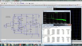
Just to let people know I've whipped up an LTspice version of Scott's 2nd, complimentary version so no-one really needs to duplicate this (the easiest one first!), and it works, how amazing, 😀! Of course, not being an amp designer, nowhere near it, took me a little bit to realise that pfets were need -- still need to insert real, reasonably accurate models of the actives, so won't post for the moment ...
Something to play with in an idle moment ... 🙂
Frank
Something to play with in an idle moment ... 🙂
Frank
Attachments
Maybe I've not been reading carefully but what are the voltage gains avalable with Scott's circuit? Is this a post volume control line/headphone amp or can it be used as a mic preamp? What are the best matched Jfets with unique gm to use? John mentioned the J113 and J175 or should it be 2sk170/J174. The first posted circuit had a + and - 30v power supply, why subsequent posts were + and - 15v? So, I assume that this has not been built with real parts on a bread board and what we see is an elegant circuit and a good SPICE simulation. Maybe a good parts list is in order. I'm ready to get the bread board out and start soldering. Thanks, Ray
You mention the "inductor trick". What is that?
See the input stage of the Jensen 990.
'using as' P channel (acting as, not changing the atomic structure, didnt I make this correction already?)
re J113: hmm no I dont think thats the fet, i'm going to have to do some more searching to see where this was discussed, one of the many threads lamenting the lack of P-channels
You may have been lost in the complementary discussions. It is typical that many devices are called complemets but in actuality they are not exact compliments. Euvl has done measurements and worked with source resistors etc. to generate more complimentary behaviour in some circuits. I beleive even after these tweaks, you are sill left with non equivalent input Cs.
> perhaps Patrick may have mentioned it....
On 2 occassions, including a recent pdf which showed measurements to illustrate that all Toshiba, Sanyo and 2N5xxx JFETs that we have tested are all D-S reversible. Don't ask me to find the link for you .......
🙂
Patrick
On 2 occassions, including a recent pdf which showed measurements to illustrate that all Toshiba, Sanyo and 2N5xxx JFETs that we have tested are all D-S reversible. Don't ask me to find the link for you .......
🙂
Patrick
You may have been lost in the complementary discussions. It is typical that many devices are called complemets but in actuality they are not exact compliments. Euvl has done measurements and worked with source resistors etc. to generate more complimentary behaviour in some circuits. I beleive even after these tweaks, you are sill left with non equivalent input Cs.
nope, its not that simple 😀 i'm aware that some compliments are more complimentary than others, the toshiba (particularly the MOSFETS) are better than most, but still many require asymmetric degeneration, to bring better, but not complete symmetry
aha!! 🙂 right OK I knew one of you had been doing some work in this area and I had an inkling it may have been you, perhaps in the initial thread for your mini jfet opamps. no worries that'll hopefully be enough info to find it. thankyou, I thought I was losing it …> perhaps Patrick may have mentioned it....
On 2 occassions, including a recent pdf which showed measurements to illustrate that all Toshiba, Sanyo and 2N5xxx JFETs that we have tested are all D-S reversible. Don't ask me to find the link for you .......
🙂
Patrick
I compliment those who use "complement".You may have been lost in the complementary discussions. It is typical that many devices are called complemets but in actuality they are not exact compliments. Euvl has done measurements and worked with source resistors etc. to generate more complimentary behaviour in some circuits. I beleive even after these tweaks, you are sill left with non equivalent input Cs.
Yes, because P-silicon has a lower mobility of majority charge carriers than does N-silicon, holes versus electrons, P devices with the same transconductance and comparable breakdown voltages must be larger than N devices. Due to those larger areas the capacitances are higher, so at high frequencies they will not be complementary --- the same behavior except for a polarity inversion. At audio frequencies, for most applications it's not as much of a limitation.
Toshiba in particular went to great lengths to make a series of very good P-channel devices, the most famous the 2SJ74, whose obsolescence is much lamented. Rumor has it that Linear Integrated Systems is working on a replacement. Wish them well.
And postscript: it's important to distinguish the drain - source reversibility of JFETs from the complementarity of specific N devices and P devices. All JFETs are, to a large extent, reversible, and some manufacturers even mention this by saying that they are symmetrical. No JFETs change their effective polarity under a swap of drain and source leads.
I've verified experimentally the reversibility of the drain - source connections of the Toshiba dual N device, the 2SK2145, which is apparently a two-chip dual using 2SK117 devices, probably plucked from adjacent positions on a wafer. Since they elected to hard-wire the two channels and use only a 5 lead package, the reversibility helps to make the part a lot more versatile. I suspect Toshiba just expected us to use it as a conventional differential pair. On earlier single-chip devices like the obsolete 2SK389, the two "source" leads were brought out, as well as a substrate connection, in a seven-lead package.
I've verified experimentally the reversibility of the drain - source connections of the Toshiba dual N device, the 2SK2145, which is apparently a two-chip dual using 2SK117 devices, probably plucked from adjacent positions on a wafer. Since they elected to hard-wire the two channels and use only a 5 lead package, the reversibility helps to make the part a lot more versatile. I suspect Toshiba just expected us to use it as a conventional differential pair. On earlier single-chip devices like the obsolete 2SK389, the two "source" leads were brought out, as well as a substrate connection, in a seven-lead package.
Just to let people know I've whipped up an LTspice version of Scott's 2nd, complimentary version so no-one really needs to duplicate this (the easiest one first!), and it works, how amazing, 😀! Of course, not being an amp designer, nowhere near it, took me a little bit to realise that pfets were need -- still need to insert real, reasonably accurate models of the actives, so won't post for the moment ...
Something to play with in an idle moment ... 🙂
Frank
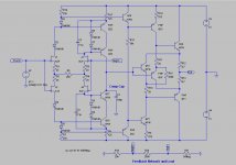
Remember to trim R18 to set the OS standing current, 8mA is enough for non-switching behavior into 600 Ohms 20V p-p
In particular the reasons for
-all the cross-coupling
- certain diodes like Q12.
- what does Q15 do and how does it do it
The cross-coupling just gets the phases right some times it's just an artifact of order drawn.
Q12, Some of the diodes just get the voltage to match across the output of diff-pairs, it can be a small effect.
Q15 just samples a voltage to drive the current sources for the output stage, this saves some devices and keeps all currents set by the input stage. It also provides a slew boost to the output devices, not much benefit here at band limited audio but it makes prettier square wave pictures😀.
Sorry about the bad JPEG conversion that dropped some 1 pixel wide lines, post #1387 has a schematic that caught this.
Toshiba in particular went to great lengths to make a series of very good P-channel devices, the most famous the 2SJ74, whose obsolescence is much lamented. Rumor has it that Linear Integrated Systems is working on a replacement. Wish them well.
I saw John Hall at the Analog Affictionados Party. They sent samples of all grades and more than one lot was represented, so it looks like there is progress. I do worry in that John is WAY past retirement and hope there are folks to carry on.
- Home
- Source & Line
- Analog Line Level
- Discrete Opamp Open Design