I'm preparing for LMG5200 based gan DDPD, bought yesterday some missing components like:
SN6505BD for isolated push pull power supplies
LMK05318B for master clock
ct7302 x two, one for anything2PCM and seccond one for PCM2DSD, between those two is ADAU1462 DSP. Project will be split into sections so each section will have their pcb. Interconnection by u-fl. DDPD will be in full brigde configuration. Volume control now from 0V to DCmax by variable SMPS.... it will be interesting project : )

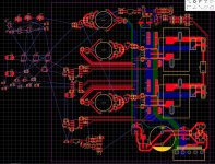
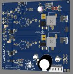
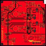
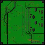
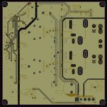
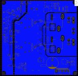
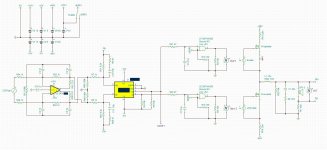
Today done some initial work on gan concept above, full bridge with ovp, ocp and dc protection. Limited to 9A. Variable power supply as a volume control from 0 to 48V. Pcb is 100x100mm
Attachments
Last edited:
Following with interest 🙂 Would the LMG5200 with a gate driver frequency rating of 10Mhz be limited to DSD128?
Yes, I don't think it can go over dsd128, I will chose dsd64 or dsd128 dependently on which one get better. : )
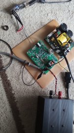
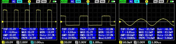
I spending some time to fix ddpd version 3, which had problem with flybuck converter, finaly solved. Now problem with dc protection, hope in next day ddpd version 3 get working. Version 3 is on fixed +-48V , no volume control based on variable psu, hmm a bit optimistic to get it work on 2.8MHz : ) Oscilograms is from MAX flybuck, isolated voltages is now all ok, Red dots is added 4.7k load resistors in paralel to capacitors. All red text is replaced values. Freq is now 207kHz and finaly an nice and clean flybuck oscilograms. The problem which is remaing now is in the DC protection which does not allow DSD to flow to the half bridge, some part of the dsd goes to the bridge but fails and the fourth is interrupted when the DC protection is activated, I have been trying to solve it for a few days, I hope it will be fixed tomorrow. It is a prelude to version 4 with variable psu as volume control which I am still holding on until I solve version 3. Version 3 is half bridge, but version 4 is full bridge...
Attachments

Last edited:
Lmg3411 have high slew rate > 150V/ns, my hope it can handle 2.8MHz@+-48V split supply, if something fail it will become puff, my hope it not happen tommorow. I'm a little scared since I need to remove dc protection temporary to make dsd bitstream non interupted. The Dsd bitstream on the complementary hi/lo will be at 2.8MHz, but the silence pattern will dominate because I will set the HQ Player volume level to -60dBFS so the bitstream will look like 0101010101... but again the fixed HV voltage is almost 100V at 2.8MHz, the lmg3411 looks like it is capable to handle that frequency and that voltage, but I not like concept of the version 3 because noise will dominate a lot because of software based volume control and fixed voltage, thats in most case expected. Let see! : ) Version 3, if I get it working, will be probably converted to ucd type class D, self oscilating, maybe I make new pcb for ucd type. In my opinion nothing close to ddpd, realistic sound, huge dynamic, instruments localization.. etc, almost everything is instant without delay. Very good sound. I will try add reclocking in ddpd version 4, thats next step. FB if even it get possible, got some idea to add current based fb trought L by adding one more wire to the output filter inductor.
Attachments
Last edited:
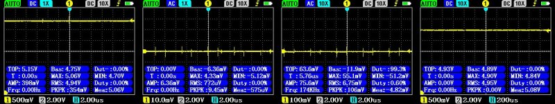
No go this day. Bypased dc protection but still other problems happening. This graf is measured before output LC, evidently is that PKPK values doesn't reach +-48V HV voltage. I hear some sounds on pcb like some pulse but didn't figured out where I hear it, graph tell everything.

Further investigating why this happen found that nErr gate sumator doesn't allow dsd bitstream to go trought, so internal protections of the LMG activates nErr sum circuity

looks like LMG is not cappable to handle 2.8MHz switching on +-48 fixed HV voltage? Too much freq??
Further investigating why this happen found that nErr gate sumator doesn't allow dsd bitstream to go trought, so internal protections of the LMG activates nErr sum circuity
looks like LMG is not cappable to handle 2.8MHz switching on +-48 fixed HV voltage? Too much freq??
Last edited:
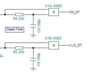
This is probably due bad circuity design for DT, probably hi/lo cross shut isue because schmit triger was missing after booth RCD : ( Isolator probably do not see corectly those 10ns dead time trought RCD. Those two signal must be reclocked trought schmit gate.
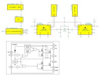
current circuity:

modified circuity for next test:

Master clock reclocking need to be implemented! What you think, what is the best way to include reclocking? Big problem for implementing reclocking is DT inclusion, what you think is the best way to implement booth DT and reclocking? I also have some idea about feedback, it can be somehow done trought implementing one more cooper coil in postfilter L and from L to an custom PLL at input complementary gates where gates might be directly reclocked trought master clock...
current circuity:
modified circuity for next test:
Master clock reclocking need to be implemented! What you think, what is the best way to include reclocking? Big problem for implementing reclocking is DT inclusion, what you think is the best way to implement booth DT and reclocking? I also have some idea about feedback, it can be somehow done trought implementing one more cooper coil in postfilter L and from L to an custom PLL at input complementary gates where gates might be directly reclocked trought master clock...
Last edited:
Don't know how we are supposed to know where you are looking at with all those waveforms.
Anyway, what is all the glitchy looking stuff in the red boxes below:

Anyway, what is all the glitchy looking stuff in the red boxes below:
Those graf is from output coil, point before coil. That glitching stufs is probably lost contact by my hand! Or maybe break by protection circuity, take a look at this graf how fast protection is, < 100ns response time. This graf is from nErr circuity, see part of the schematic for idea about nErr sum on U11 AND gate, there is 3 protections routed, nErr is on the folowing graph.

I will try to increase dead time on rcd network by changing 100 ohm with something < 1k, if that help than in that case DT is the only problem. Curently I have no idea why protection is activating because components is 0603 and I do not have free space to put sond and measure by two channels booth hi/lo . Voltages is dangerous to risk by hand : ) Graf above is without spring on sond, it looks much cleaner when spring is used but can't do it by spring because of soo thin components and things close to bridge, no want to risk my face and hands : )
I will try to increase dead time on rcd network by changing 100 ohm with something < 1k, if that help than in that case DT is the only problem. Curently I have no idea why protection is activating because components is 0603 and I do not have free space to put sond and measure by two channels booth hi/lo . Voltages is dangerous to risk by hand : ) Graf above is without spring on sond, it looks much cleaner when spring is used but can't do it by spring because of soo thin components and things close to bridge, no want to risk my face and hands : )
Last edited:
It's a little scary at that voltage, Hypex smps fixed +-48V, I can hear a sound on the pcb like a clicking sound before the protection stops the board from probably exploding. : )
Last edited:
Need DSDOUT in dsd64! Is this ok reclocking mechanism? DSDIN is always in dsd64 too, need to reklock it and found idea maybe 8bit shift register can do things perfectly well using those two oscilators? Freq/8 excatly 8 cicle until next dsd input bit fill Q0...Q7 ?
Attachments
Last edited:
Reclocking is usually done to reduce accumulated jitter. Is that what you want to do, or is what you really want to do is more like to delay the clock to better align it with the rest of your system?
I want to align the hi/lo pulse width against the ref freq based on 44.1k or 48k. The above mechanism that I drew with the shift register is interesting and maybe it could work, but in that case the ct7302 would also have to be synchronized with the clock, that is already too complicated for me since I use it asynchronously, without synchronising ct7302 it is not possible to do this reliably via shift register, for example if dsd_in were just a little late or a litle later things would not work right, probably an unexpected bit would be pushed into the shift register. I have no idea how to do this mclk/8 reclocking so that the clock prevails on hi/lo and dsd_in is only a guideline to which gate the pulse from the clock will be forwarded. Than to that need to implement deadtime on booth hi/lo. Dead time I will do trough AND gates and simpe rc network thats easy to do, but reclocking is now problem to dsd64 from dsd512 oscilators. Isolators and things is not problem because of prety close cross-channel delay, but only now reclocking is isue, have no idea how to do it.
Dead time I'm thinking to do with varactor diode + i2c cntroled 16bit dacs, that would make the later setup work much easier. : )
Dead time I'm thinking to do with varactor diode + i2c cntroled 16bit dacs, that would make the later setup work much easier. : )
Attachments
Last edited:
For a dac to work properly the time reference has to be exact as possible. You can't go around estimating the timing and adjusting it arbitrarily to make your circuit work. You have to do it the other way around and design the circuitry to work with the required clock timing. If that means you need to synchronize the CT7302 than that's the problem you should be focusing on.
- Home
- Amplifiers
- Class D
- Direct Digital Power DAC (DDPD)