I need somebody so gentle to validate my schematic at post #46. It derives from the "Baby Huey" in this thread:
Let it be clear that it must supply a driving signal of at least 60Vp per phase with 1Vp at its input.On a couple of threads I have promised to post the schematic for my latest (and best) version of my EL84 Ultralinear Amp. This design is based upon an ECL86 Amp design posted by Yves quite some time ago. This design uses shunt feedback to reduce the output stage rp and thus better drive the limited primary inductance of cheaper output transformers. Regardless of that, the result is good enough that its worth using reasonable quality transformers and while the common Hammond 1608 (Raa = 8K) will work well, it really deserves something a bit higher quality (more expensive). It can be used...
- gingertube
- Replies: 2,774
- Forum: Tubes / Valves
I will build it balanced because this is the shortest way for me to hear its sound. I will connect it as a front end to a cyclotron mid-power buffer back end I already have. Its present front end is a buffered DC coupled Concertina, Williamson style, which I wish to improve.
With the DTB I intend to build, only one phase will be used, and its design is now clear (even if the servo is not that clear). Once I obtain the sound I wish, this front-end will be simplified as unbalanced, without a negative power supply. Maybe some ECLxx can be used as a single tube for 1st (high mu) and 2nd (high transconductance - as a triode) stages with a +b=250V, but I'm in doubt if the 60Vp can be obtained.
Thank you!

I'm attaching a marked up schematic from post 15 depicting a DC servo I believe can be well damped. But I thought I should ask about the eventual scheme, as the servo may not be appropriate to a Circlotron implementation.
Re the post #46 design, I still imagine the single phase variation might be made to work if you're willing to incorporate negative feedback. (I have suggestions if so.) I think the bootstrapped drive is a step in the right direction, and retaining the constant current load on the MOSFET buffer would help. What device type do you intend for the FETs? In any case, you should expect similar problems in both top and bottom sections of a two-phase design.
In your diamond buffer schematic, I'm suggesting an added pot and two resistors (R5,6,7) in lieu of R104 and R105. If you ground the wiper of R6, I think you might be able to avoid using the DC servo. Alternately, the post jumper depicts the option to enable DC servo. The servo amp includes R1, which is necessary to accommodate the slow response to changing the bias voltage across C101, C102. This is a very typical measure to adjust loop damping.
If this general approach appeals, I'll finish analysis and provide details about component values, adjustment procedures, etc.
Last edited:
@marigno
i've been following this thread and was looking to play around with this circuit. pardon my ignorance, i am not an analog wizard, but..... how do you get reasonable voltages out of this configuration? it feels to me like R2 will ALWAYS see the +Vbe and -Vbe to bias the power transistors and set a very large standing current in R2 and the respective Q8/Q9. i gotta be missing something :O

i've been following this thread and was looking to play around with this circuit. pardon my ignorance, i am not an analog wizard, but..... how do you get reasonable voltages out of this configuration? it feels to me like R2 will ALWAYS see the +Vbe and -Vbe to bias the power transistors and set a very large standing current in R2 and the respective Q8/Q9. i gotta be missing something :O
Hi drinkingcube,
Look at the Vbe drops.Q7 base is near the common voltage, Q7 emitter is one Vbe, then you hit Q8 and a Vbe drop the other way. They nearly cancel. Same for Q6 and Q9.
Several very good commercial amplifiers use this basic circuit. It is very stable as well.
Look at the Vbe drops.Q7 base is near the common voltage, Q7 emitter is one Vbe, then you hit Q8 and a Vbe drop the other way. They nearly cancel. Same for Q6 and Q9.
Several very good commercial amplifiers use this basic circuit. It is very stable as well.
I echo anatech's comments.
The standing current through R2 is set approximately by the voltage from the bias diodes V1 and V2--- about 2 Vbe.
But your other observations are also correct. The circuit has ~ unity voltage gain, so the input signal has to swing rail-to-rail to drive the the output to full power. The I1, I2 current sources also are a challenge when the signals approach the rails and head-room voltages shrink to minimum. Simplest is probably implementing them as boot-strapped current sources---
eg. two series-connected resistors between Q7's emitter V+ with the bootstrap capacitor to the out terminal. Similar for I2.
Cheers.
Another solution seen with Mosfet amplifiers is to run the voltage amp stage from higher regulated supplies. This has other advantages as well.
Look up the Marantz 300DC. Regulating the voltage amp means that power output has very little effect on what the voltage amp is doing.
Look up the Marantz 300DC. Regulating the voltage amp means that power output has very little effect on what the voltage amp is doing.
@anatech @BSST
thanks for the comment guys. everything you made sense to me, i totally see how the vbe drops cancel and the two pairs of transistors float with the signal voltage that is common to them. whats left at the emitters of Q8/9 is the remaining bias voltage for the output pairs. my last point of confusion:
is the value of 33 ohms for r2 incredibly low? in my sim there is 39.9 mA through it (-749 - 561 / 33) and that seems unreasonably high, as it makes Q8/9 run at a power level that would instantly blow them up in real life.
thank you again for the discussion/clarification
Normally those transistors are mounted on a small heat sink along with Q6, Q7. That stabilizes bias current.
I assumed the devices were there for a quick simulation.
Have a look at how amps similar to this are built physically. There are things not shown in a schematic necessary to make a reliable amplifier. Thermal coupling is important. Really important. Proper device selection of course. That is the engineering part of circuit design.
ok. i'll look up the Marantz 300DC and see what they're doing there. i understand also how thermal stabilization would work here, but i also believe that in a single shot LTSpice transient sim, DC conditions should look how they should before thermal effects start altering things. i.e. i'm looking at the signal over 10 cycles, i think the conditions i'm looking at should be valid. yeah, i'm wondering if 33 ohms was a placeholder value but i'm not entirely sure. again, i will look up the marantz and see what they're up to there. appreciate it. thanks 🙂
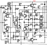
R749 24 ohms at 25 mA (0.6 / 24 = 0.025)
Q713 VCE at 69.4 (70 - 0.6 = 69.4) at 25 mA is 1.735 Watts ... seems insanely high but it's the same thing that @marigno is doing. is the thermal feedback that powerful? i.e. it will settle quickly and not kill Q713? i thought the whole point was to avoid 1.725 W in Q713 and that diamond buffers allow both pre-driver and driver to be small signal TRs.
Attachments
Thermal time constants are much longer, like over 10 minutes. Simulators aren't very good here and mostly lie.
When you are sim driving, keep in mind the simulator assumes all components are exact on spec, and exactly the same. This is completely unrealistic. The models are pretty simple on average, and some are not even made using empirical data (fantasy parts). Never mind thermal effects and traces. A minor detail of where a part is on the PCB, plus what it may be thermally coupled to makes massive differences.
There are thousands of Marantz 300DC amplifiers out there, Nakamichi 620 and others. They are reliable and all have good reputations. I don't see many for service in the Toronto area, and this is a hot spot for audio. I have three Marantz 300DC amplifiers. They can fail but the worst damage comes from people trying to service them. Same for any product really.
i think i figured out my misunderstanding. there's no way to get around the fact that the transistors in the second half of the diamond buffer (the drivers - if we're doing pre-driver, driver, and outputs) needs to be a beefier transistor as, yes, the bias conditions in the simulation i've been seeing match what i'm seeing in other schematics with a similar topology. i was misunderstanding that the driver can also become a small signal transistor but now i see that it still has to have the same driver transistor characteristics to deal with the required power consumption.
Yes. Not only that, but it has to properly mount to a heat sink to thermally couple to the other parts.
Have a careful look at how the Marantz 300DC, or 1180DC goes together physically to get which parts are coupled. There are more models, but these two examples should show you enough. They are TO-126 parts and happily they lend themselves to being screwed down to something.
Have a careful look at how the Marantz 300DC, or 1180DC goes together physically to get which parts are coupled. There are more models, but these two examples should show you enough. They are TO-126 parts and happily they lend themselves to being screwed down to something.
@BSST
This is a busy and messy time for me, trying to be after too many things to do. I could find a "time spot" to post just now.
My project is the DTB, but I also have a Circlotron ideally in two cabinets: VAS/phase splitter in one cabinet, and Circlotron buffer in the other cabinet. Actually, they are in 4 cabinets (dual mono/dual body) but this is another story. That's why I drew the VAS for the DTB as a VAS/phase splitter (even because the double triode tubes would be used half). The Circlotron is here https://www.diyaudio.com/community/...-a-hybrid-main-amplifier.396135/#post-7276068 and I wish to try a different front-end. BTW, its offset is rock solid zero with no servo.
Let's forget the Circlotron and focus only on the DTB. The VAS will be something like the schematic here attached.
The DTB schematic is clear, the only thing to finalize is the servo.
I wish not to use a servo, but, when you design, you must not neglect it. So your mod to the schematic is very welcome. It is the right one, and the damped servo is too. Would you like to give the values for R1, R2, C1, C2, please?
Let's look at the schematic here enclosed, which is almost definitive: a CCS in place of R221, as a load for the MOSFET, is nullified being around 4KΩ the load seen by the MOSFET itself after C212, without considering R221.
I haven't decided yet whether to use a global feedback loop. I'd vote for no feedback. If yes, I need to connect a resistor around 50 x R213 from the DTB's output to the cathode of V211; this means a 3rd cable from one cabinet to the other.
Attachments

Just an idea for your inspiration in case you are into fancy and risky circuitry,
Perhaps you have an idea inspiration for a powerful solid state input stage with a phase splitter?
so that there is 1 volt at the input, and 60-70 volts at the output of the phase splitter, at extremely low TND
even if using op-amp
- Home
- Amplifiers
- Solid State
- Diamond triple power power buffer