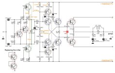
I'm studying a buffer to drive a couple of speakers. The buffer is to be driven by a mu-follower. There will be no signal feedback loop.
I wish to achieve an output power of around 200W.
After reading Bob Cordell, I chose the diamond triple topology.
My concern/doubt is as follows:
I drew only one final pair, there will be more.
Any help would be appreciated.
I wish to achieve an output power of around 200W.
After reading Bob Cordell, I chose the diamond triple topology.
My concern/doubt is as follows:
- C103 (red), to be used in a triple Darlington to speed up the final pair to switch off, perhaps it should not be used with this project;
- the xVbe (components with index 5xx - it is needed a temp sensor and 2 x Vbe to compensate the final pairs) with its CCSs; perhaps a simple series of 2 diodes (component index 7xx) hits the spot, and the two CCSs made out of depletion mosfets are not needed anymore;
- the point where to apply the DC feedback (servo) to maintain the offset at zero, I'm not particularly eager to use a servo connected to the input, because it will interact with the input capacitors, so I'm trying to connect the servo to the CCSs feeding the folded EF.
I drew only one final pair, there will be more.
Any help would be appreciated.
Attachments

A Diamond buffered triple EF is probably the best thing I've ever built.
Capacitor C103 can be used, no problem. Why do you suspect issues?
Thermal compensation is super easy: Just thermally couple T102 to T105 and T103 to T106.
I used a very basic Vbe multiplier attached to T107 and T108 - works very well.
Are T503 and T504 meant for DC offset correction?
Capacitor C103 can be used, no problem. Why do you suspect issues?
Thermal compensation is super easy: Just thermally couple T102 to T105 and T103 to T106.
I used a very basic Vbe multiplier attached to T107 and T108 - works very well.
Are T503 and T504 meant for DC offset correction?
Thank you for the suggestion about C103. It has a 1µF value, not 100nF, I made a typo. I'm concerned about its interaction with the collectors of the predrivers configuring a 33µS TC (4823Hz).
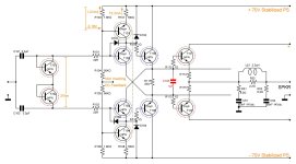
T503 and T504 are CCSs meant to feed the xVbe and should be thermally coupled among themselves.
When coupling the predivers and drivers you only sense the drivers' temperature, not the final pairs' temperature. In the design of a 200W amp, it is mandatory to sense the temperature of the final pairs.
I'm evaluating a better idea about the xVbe, which doesn't need any CCS (T503, T504): a series of two transistors (T701, T702), perhaps the same as a final NPN transistor, connected as diodes, mounted on the same final pairs' heat sink.
The most important concern, now, is the connection point of the servo output. This project is a buffer, not an amp, therefore there is no easy point to connect the servo. I don't want to connect it to the input, after the capacitors. This is why I didn't use a fixed voltage to polarize the CCSs' bases; I used resistors (R103, R106) instead of diodes. When the servo shows 10V at its output, only 300mV variation shows on the CCSs' bases, which will determine a 0.3mA difference to each predriver. Will this be enough to correct the offset? It seems yes, but at the same time too simple, I didn't see such a solution in other schematics.
Here is an updated schematic.
Where did you connect the servo?
Attachments
I understand your concern about interaction of the red capacitor with the driver's collectors. Maybe consider series resistors for those collectors, just as an option. Bootstrapping the collectors like you do is great, but prone to gain peaking. You may want to investigate this in detail and experiment with bespoke resistors. BTW: I believe we mixed up reference designators: C105 is red, not C103. I was talking about the red capacitor all the time.
Ah, I see the green dotted connection now. Can't say anything about this though.
You have a pretty sophisticated Vbe multiplier using a CFP. What is the rationale behind?
A basic Vbe multiplier thermally coupled to the power transistors works well for me.
I would be afraid of the CFP becoming unstable.
The big advantage of the diamond buffered triple is super easy thermal compensation. As you pointed out, pre-driver and driver are out of the equation. Just the power transistors need compensation, regardless of output power.
Can't say anything about the servo, because my triple was enclosed in a global feedback loop.
The updated schematic with T701 and T702 seems a bit borderline to me because the current through those two transistors is likely very small (base current of T102 and T103). In the previous schematic, you have 10mA through the Vbe multiplier, which is solid.
You are right, the capacitor I'm talking about is the red C105.
The bootstrapped collectors solution is present in Bob Cordell's book, he says as follows:
"The collector voltages of the folded emitter followers move with the signal because they are bootstrapped by the signals at the emitters of the opposite driver transistors. This mitigates the nonlinear effects of their collector-base capacitances on the VAS output node. The Early effect in the predrivers is also greatly reduced. This arrangement permits the use of fast, low-voltage transistors for the predriver. Power dissipation in the predriver is also much smaller. Most of the dissipation that was once in the predriver is now in the current source, whose signal characteristics have little influence on the signal path."
My precedent diamond triple doesn't use this topology, the predrivers' collectors are connected directly to the power rail.
The xVbe with CFP was an old idea of mine I applied already, and it didn't oscillate. I found it again in the last few days while reading Cordell and copied here the same I made in my last amp. R506 prevents it from oscillating. But there is another problem: this kind of xVbe increases the voltage at its ends when the power voltage changes: with a low voltage the bias on the final pairs is high, with a high voltage the bias is lower. So, perhaps, the two diodes could be the solution. As you say, a higher current must flow inside them, I should revive the two CCSs made out of depletion mosfets or (better I think) use a couple of 100KΩ resistors allowing 0.7mA to flow, which should be enough. I wish to avoid the simple xVbe because it too modulates the bias depending on the power voltage. Perhaps the simple and the CFP xVbes work well when 6 x Vbe is needed as in the Darlington triple. The two-diode bias spreader has the good point of tolerating an unstabilized power supply.
The entry point of the servo remains still the main issue.
Bob is right, it seems to have only advantages to bootstrap.
A third option would be to bootstrap to the output node directly.
See figure 11.16 in his book (1st edition) "A MOSFET output stage with folded drivers".
Works with BJTs, too, and in this case the bias generator could be left away since what he calls "folded drivers" is actually a Diamond configuration.
If you are unsure, you could have all three options using resistors that can be installed or left away (a bit tricky though).
Implementing only two options (rail or bootstrapped) is trivial however and may save you from a PCB re-design.
Bootstrapping is super nice, but comes with potential instability.
I observed severe gain peaking in bootstrapped Diamond Buffers.
This can be tamed with resistors in series with the pre-drivers collectors (hint from someone here on the forum), which need careful optimization for best performance.
I can't really follow you with the Vbe multiplier.
Power voltage is the signal voltage?
Resistors instead of CCS means that the current modulates with signal swing, not the best choice in my opinion.
I haven't investigated Vbe multipliers at all.
What I use is like figure 14.9b in Bob's book.
This is a an interesting project and I can't resist weighing in. 😀
Your jpg in post in post 3 is intriguingly simple. If the Beta of T102 and T103 is about 100, the base currents would be about. 150uA. If you inserted a trim pot in series with the T701/T702 pair, might 150uA be sufficient?
About applying servo bias:
It appears to me that mismatch in Beta of T102 and T103 is a challenge--- let's assume 10% mismatch, or about 15uA. The input impedance of the circuit is very high and not well defined, and bias current mismatch would be a huge uncertainty of input bias voltage. But your mention of 100K resistors suggests that 50k load or larger would be acceptable?
In an earlier post, you implied +/- 10V for servo drive. 10V/15uA= ~670k. So a pair 1.3M resistors tied across the T701/T702 pair and tied to servo opamp would be my suggested approach for servo injection. The time constant of these resistances and the C101//C102 caps has to be accommodated in the servo design, but that's easy. And the 1.3M can of course be made smaller.
Let me know if this unclear,
Last edited:
@Lee Knatta
@BSST
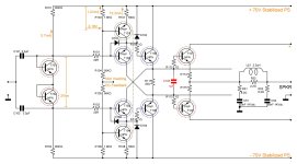
What I meant is in this schematic, R701 and R702. The schematic is far better than my bad explanation.
Cordell's Fig.11.16 cannot be easily adapted to BJTs, the two CCS must feed a far higher current, being the current available on the load is strictly dependent on the two CCSs. On the contrary, the triple allows a low current from the two CCS which will result in a high current available on the load, far over the needed current.
Three years ago I built a 200W diamond amp named WHA-217, it is here: https://www.diyaudio.com/community/threads/dartzeel-amp-schematic-build-this.134362/page-106 - post #2107 and following. It performs very well, I love its sound. But once again it has the servo problem. The servo produces some subsonic artifacts. It is a non-inverting servo, which should be avoided.
I wish to use an inverting servo, but I cannot find a good point of injection.
I suppose the injection point I put in the schematic could be a good solution, but again I need a non-inverting servo. This time I'm not going to use the simple non-inverting solution, but the inverting servo followed by an inverting buffer (Cordell's fig. 8.5).
The bootstrapping of collectors is a secondary aspect because I have the solution ready, I can use it or I can connect the collectors to the power rails. Or use the optimization technique you cited.
The xVbe also is almost a resolved issue, I think this last schematic will be good, and will not overload the VAS I intend to use, a hybrid mu-follower with a very low output impedance.
I'm not concerned with the strict selection of components: the WHA-217 without connecting the servo shows 1mV offset by itself, slightly drifting with the temperature.
I will avoid for sure to connect an inverting servo to the input (right side of C102, C102), I am supposed to adjust the value of C101, C102 also depending on the impedance of the source. This is not a good way.
So the question is still open: is the named "Non-Inverting DC Feedback" a good injection point for a non-inverting servo? I didn't see this solution elsewhere, and I'm not known to be an expert.
Thanks to both of you, you made me think!
@BSST
What I meant is in this schematic, R701 and R702. The schematic is far better than my bad explanation.
Cordell's Fig.11.16 cannot be easily adapted to BJTs, the two CCS must feed a far higher current, being the current available on the load is strictly dependent on the two CCSs. On the contrary, the triple allows a low current from the two CCS which will result in a high current available on the load, far over the needed current.
Three years ago I built a 200W diamond amp named WHA-217, it is here: https://www.diyaudio.com/community/threads/dartzeel-amp-schematic-build-this.134362/page-106 - post #2107 and following. It performs very well, I love its sound. But once again it has the servo problem. The servo produces some subsonic artifacts. It is a non-inverting servo, which should be avoided.
I wish to use an inverting servo, but I cannot find a good point of injection.
I suppose the injection point I put in the schematic could be a good solution, but again I need a non-inverting servo. This time I'm not going to use the simple non-inverting solution, but the inverting servo followed by an inverting buffer (Cordell's fig. 8.5).
The bootstrapping of collectors is a secondary aspect because I have the solution ready, I can use it or I can connect the collectors to the power rails. Or use the optimization technique you cited.
The xVbe also is almost a resolved issue, I think this last schematic will be good, and will not overload the VAS I intend to use, a hybrid mu-follower with a very low output impedance.
I'm not concerned with the strict selection of components: the WHA-217 without connecting the servo shows 1mV offset by itself, slightly drifting with the temperature.
I will avoid for sure to connect an inverting servo to the input (right side of C102, C102), I am supposed to adjust the value of C101, C102 also depending on the impedance of the source. This is not a good way.
So the question is still open: is the named "Non-Inverting DC Feedback" a good injection point for a non-inverting servo? I didn't see this solution elsewhere, and I'm not known to be an expert.
Thanks to both of you, you made me think!
Attachments
Shame on me!
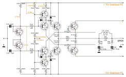
the servo injection point I put on the schematic is wrong, it makes no difference in injecting the servo (inverting) to the bases of T102, T103.
Here is why: let's look at only the upper half of the schematic for simplicity.
Imagine a negative signal of 10V from the servo. It will move the voltage on R103 by about 300mV (from 2.18 to 2.48), so the current on T101 will increase from 15.3mA to 18.3mA, a 3mA difference. T101 tries to pull the emitter of T102 for 3mA more, but it cannot move at once because its base is kept stable by the TC determined by C101, R701, and the output impedance of the VAS. When the TC is past, it will result in the same overshoot we would see connecting the servo to the bases of T102, T103.
Sorry for bothering you, this problem doesn't seem to have any good solution.
Hi marigno,
I looked a bit earlier at your design and became convinced it would work as you suggested. I remain convinced still.
I have a chore that I can no longer avoid, but will return eventually to present my argument. A short comment is that the input time constant is 100k//100k * 3.3uF/3.3uF = 0.33sec. The input won't respond instantly, but it will given settling time.
Be of good cheer! I think your proposal will work as you intend.
Here's my contention that your adjustment scheme will work as you intend:
Initially, let's assume well matched transistors and the servo injection is set to 0V. Then transistors currents will be as you've noted in post 8. With matched Beta, the base currents through R101 and R102 will have identical magnitudes, yielding net 0 current into the R701, R702 bias string. The input T701/T702 pair will be balanced at +/- 0.6V, and the buffer output will be 0V.
Now let's assume T103 has Beta of 100. Base input current is 15.3mA/100 = 150uA, into the base. But assume T102 is mismatched 10% re T103 and has Beta = 110. Base current flowing out of T102 is 15.3mA/110 = 139uA, an imbalance of 11uA that will pull the bias string negative by 11uA * 50K = -0.55V. The buffer output will be about -0.55V.
Now as you suggest in post 9: "Imagine a negative signal of 10V from the servo. It will move the voltage on R103 by about 300mV (from 2.18 to 2.48), so the current on T101 will increase from 15.3mA to 18.3mA, a 3mA difference." In similar fashion, the voltage across R106 will move from to 2.18 to 1.86, a drop of about 311mV and a decrease of T104 current from 15.3mA to 12.3mA. (The net change in T101-T104 transistor currents is about 6mA and has to flow toward the buffer load.) So now the base current flowing out of T102 base is 18.3mA/110 = 166uA and base current flowing into T103 is 12.3mA/100 = 123uA, a difference of about 43uA that pulls the bias string 43uA * 50k = 2.15V, a shift of the input to positive positive voltage of the T701/T702 pair.
I believe this demonstrates the servo injection node has plenty of control range. I think your control scheme will behave as you hope. If you disagree, I welcome discussion.
Nice work!
Imagine shorting the input, shorting C101, C102, and neglect the bias diodes. Varying the current on the emitter of T102 does not affect moving T102 because its base is solid (its collector is eventually bootstrapped, but imagine it is connected to the negative rail, so the collector is out of the question). Now put in place C101, C102, and consider the TC. T101's base can now be moved with a delay imposed by the TC multiplied by its β (let's assume this is correct, even if not precise). So the settling time would be βTC (the day after!). Injecting the servo (inverting) after C101, C102 is better because T102's β is not to be considered.
The point R104/R105 could be used to fine-trim the offset compensating some tolerance in components like you say, but it is a static correction and we do not need the servo for this purpose. But, again, it will not work if you short C101, C102.
This diamond buffer cannot be used without coupling capacitors at its input, which is not a negative point.
The solution to the optimal servo injection point seems to be unsolvable.
Perhaps, on the contrary, a very slow settling time is what is needed, because the offset will vary slowly with the temperature. In this way, the overshot of the servo interacting with the TC is avoided because it interacts with βTC.
A static pre-regulation to zero the offset with the servo disconnected is still needed, but simple to achieve.
I put myself in a no-way-out corner.
A static pre-regulation to zero the offset with the servo disconnected is still needed, but simple to achieve.
I put myself in a no-way-out corner.
It can work with BJTs and I experimented with this. CCS were set to 100mA and driving four pairs of BJTs output stage.Cordell's Fig.11.16 cannot be easily adapted to BJTs, the two CCS must feed a far higher current, being the current available on the load is strictly dependent on the two CCSs. On the contrary, the triple allows a low current from the two CCS which will result in a high current available on the load, far over the needed current.
Current gain is rather low of course, which makes this arrangement less compelling - like any dual emitter follower.
Bias is also on the high side with BJTs (class A operation only) and cannot be brought down to class AB. Doesn't matter much for a driver though.
But basically it works.
I meant this for illustration for another way to bootstrap only.
This kind of diamond buffer can be used in a triple as well.
I believe the bootstrap you are planning to use is a good choice - more flexible and a bit less difficult to optimize.
However, the bootstrap shown in figure 11.16 can attain very low distortion, lower than the bootstrap to the emitter resistors of the power BJTs.
It is according to what @Lee Knatta said in #14 post: bootstrapping both predrivers (R211s) and drivers (R801).
Hm, well, this is not what I meant.
Not sure what R801 will do.
Aren’t the drivers bootstrapped to the output node anyway?
I was referring to the pre-driver to driver bootstrap.
It would be possible to bootstrap the drivers collectors to the output, but this is complicated and prone to instability.
Not sure what R801 will do.
Aren’t the drivers bootstrapped to the output node anyway?
I was referring to the pre-driver to driver bootstrap.
It would be possible to bootstrap the drivers collectors to the output, but this is complicated and prone to instability.
You're right, my last schematic can't work. Or better, I don't know, I should study it. I want to use a triplet, probably it would be possible to bootstrap the collectors' predrivers to the final pair, but I never saw such a schematic. I would not bootstrap with the second next stage with a stage in the middle.
Here is how the bootstrapped drivers collectors could be implemented basically:

Just an idea for your inspiration in case you are into fancy and risky circuitry, I'm not suggesting to implement this.
This comes with some benefits and issues, not sure whether the benefits outweigh the issues.
Just an idea for your inspiration in case you are into fancy and risky circuitry, I'm not suggesting to implement this.
This comes with some benefits and issues, not sure whether the benefits outweigh the issues.
- Home
- Amplifiers
- Solid State
- Diamond triple power power buffer