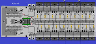
Dx Custom is the name and i am starting to make it
Here you have a video...next video today.
Dx Custom - YouTube
regards,
Carlos
Here you have a video...next video today.
Dx Custom - YouTube
regards,
Carlos
we wait for the final scheme....regardsIt almost ready to 4 ohms loads...more than 700 watts RMS at 35 hertz with less than 0.6% distortion.
To the ones are preparing pcboard:
Supply rail condensers are huge...left side (input side) is 1000uf/100V and to the right side we have 2200uf/100V...they are big in size...and soon they gonna have small capacitor in parallel...circuit is not ready.
The heat sensor diodes are high speed TO220 devices, made of plastic (have plasticity, you can make shape with that material) and the internal junction is electrically insulated from the heatsink.
I will try big transistors (output units) as drivers and maybe as VAS...so...it is not a good idea to prepare pcboard for a while.
regards,
Carlos
Dx Custom give up... the powerfull amplifier for bass is not that powerfull
Was not approved.... a video explains:
Dx Custom not approved! - YouTube
regards,
Carlos
Was not approved.... a video explains:
Dx Custom not approved! - YouTube
regards,
Carlos
Yes... he is very good...also his videos are nice
You will not believe if i say he made an overhaul of his old Toyota Corolla.
This guy knows what is good...first the Toyota Corolla and second a Dx amplifier😉
His hands are magic.
regards,
Carlos
You will not believe if i say he made an overhaul of his old Toyota Corolla.
This guy knows what is good...first the Toyota Corolla and second a Dx amplifier😉
His hands are magic.
regards,
Carlos
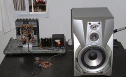
Well I have the heat sink ready, for now I just design a new power supply "simple" not complicated and is unregulated, I took the idea from a eBay power supply that look interesting so I making my own one, is a double side board and I'm going to try etching it but I need to get me a laser printer first lol 😀 hey guys if you have any ideas that can you share with me let me know. 😉
Regards
vargasmongo3435
Regards
vargasmongo3435
Attachments
Last edited:
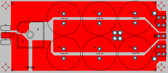
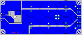
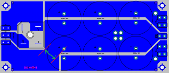
you need a connection for the centre tap at the rectifier end of the capacitor bank.
I would also "neck" (narrow) the common ground strip between the first pair of caps and the second pair. This may help reduce the charging pulses that will try to travel towards the output in search of the lowest impedance.
I would also "neck" (narrow) the common ground strip between the first pair of caps and the second pair. This may help reduce the charging pulses that will try to travel towards the output in search of the lowest impedance.
the board is double side, the center tap is already connected to the center of the board, the red is the top side of the board and the blue one the bottom but if I'm wrong I will check it again, when you refer to "narrow" is the blue one or the red one that has to be change it to avoid the pulses? 😕
Regards
vargasmongo3435
Regards
vargasmongo3435
Attachments
Last edited:
Thank you Alex... sadly this amplifier was not approved
But this remote output, we can use with several amplifiers, will be alway usefull.
Also thank you by your kindness Juan.
I am playing with that non approved prototype.... using filters and playing with it...soon i will upload a video...a bad quality video but shows the unit working.
http://www.youtube.com/watch?v=TqJWYTNA6KM
regards,
Carlos
Attachments
Last edited:
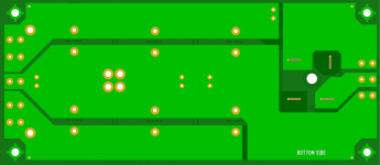
Don't mind the not connected fuses the prototype was not approved dear Alex that is why I is not completed, and I just want it to show where did I stop the layout.
Regards
vargasmongo3435
Regards
vargasmongo3435
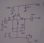
Juan. here you have the circuit i am using to "play with bass"
That is the subject of this small movie here:
Playing with bass - YouTube
If you want to make it, or to produce a layout...then i am posting the schematic.
regards,
Carlos
That is the subject of this small movie here:
Playing with bass - YouTube
If you want to make it, or to produce a layout...then i am posting the schematic.
regards,
Carlos
Attachments
Herman is having fun with uncle charlie.... he sent me this picture
Crab is an animal that walks backwards...this means he do not advance to the future..he return to the past...and Dx amplifier is past...old amplifier already made.
Hehehehehe...he is right.... does not make sense to go "forward to the past" nor back to the future.
regards,
Carlos
Crab is an animal that walks backwards...this means he do not advance to the future..he return to the past...and Dx amplifier is past...old amplifier already made.
Hehehehehe...he is right.... does not make sense to go "forward to the past" nor back to the future.
regards,
Carlos
Attachments

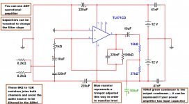
Returning from job in the afternoon i will continue to play
Will try to modify the bass slope.
regards,
Carlos
Will try to modify the bass slope.
regards,
Carlos
Attachments

Last edited:
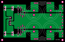
move the centre tap connection the space right next to the rectifier......................... the center tap is already connected to the center of the board, the red is the top side of the board and the blue one the bottom but if I'm wrong I will check it again, when you refer to "narrow" is the blue one or the red one that has to be change it to avoid the pulses?................
Remember the charging pulses run around the circuit from secondary/rectifier/first+ve cap/centretap/secondary/rectifier/first-ve cap/centre tap and repeats on every cycle. You don't want the traces carrying these pulses (in a figure of 8) to be shared with any circuit downstream of the charging circuit.
Look at the area between the first 4 smoothing caps.
There is a very wide Zero volts trace running from left to right through that space. Narrow the trace to maybe 5mm wide. This will help keep the charging pulses to the left side of the narrowing. Then the Zero volts side to the right of the narrowing will have much less of the charging pulses imposed on it. That should help "clean up" the output side of the PSU.
V,
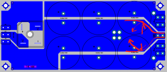
the +ve rail trace and the -ve rail trace connecting all the like poles of the smoothing capacitors can be improved.
Break the +ve trace between the first cap and the second. Break the +ve trace between the second cap and the third cap.
repeat this for the -ve side traces. And repeat on top and bottom sides.
Insert pads to allow shorting links to be soldered in to maintain trace continuity from transformer end to the output end.
Now the OPTIONAL improvement:
replace the first +ve link and the first -ve link with radial resistor that fits the little gap at the edge of the PCB.
This changes the PSU from rCCC to rCRCC.
The second OPTIONAL improvement:
replace the second +ve link and the second -ve link with radial resistor that fits the little gap at the edge of the PCB.
This changes the PSU from rCRCC to rCRCRC.
The R can be any value dependant on current demand. I'd suggest the quiescent Vdrop across the first resistor be <300mVdc and across the second resistor <100mVdc.
You can replace these resistors with air cored handwound inductors with a R value (the copper wire resistance) ~ = the the R value that gave those same voltage drops I suggested above.
For a little amplifier say ~100W (Iq~100mA) the resistors could be 0r33 (1st) and 0r22 (2nd)
for a big amp say 300W (Iq~600mA), the resistors could be reduced to ~ 0r22 & ~ 0r1
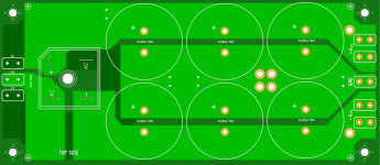
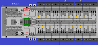
Hi Carlos and hi all,
i designed this pcb from your schematic;
Greg's Web Site
and inspired from this pcb design;
http://www.diyaudio.com/forums/group-buys/187592-3-symasym-21.html#post2866591
just want to be sure before etching if it has any error or fine to go?
thanks..
i designed this pcb from your schematic;
Greg's Web Site
and inspired from this pcb design;
http://www.diyaudio.com/forums/group-buys/187592-3-symasym-21.html#post2866591
just want to be sure before etching if it has any error or fine to go?
thanks..
Attachments
Last edited:
- Status
- Not open for further replies.
- Home
- Amplifiers
- Solid State
- Destroyer x Amplifier...Dx amp...my amplifier