Greg, I couldn't get the other files our dutch friend posted to open... you don't feel like shareing your's maybe?
Now for something else...
I never knew a transformer could be responsible for channel seperation....
I am doing some fault traceing on the little mosfet headphone amp I built... very basic... single mosfet, some resistors and some caps each channel...
the 2 channels are completely seperate, only connected to each other at the ground point on the headphone sockets...
The power supply is 1 per channel, each driven off its ow secondary winding from the same transformer...
Anyhow testing with one channel not powered , I could clearly hear the sound comming through from the other channel...
Not sure how.... but yeah it was revealing in that things were obviously not as seperate and simple as I thought... adjusting bias on one channel, affects the other too!!!!!!!
So from now on I supplose its time for seperate transformers...I still think I may have been haveing a brainfart, and the source of the second signal will hit me over the head when I wake up all the way.
Hi Roender.
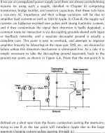
My star ground point would be (is) on board between the decoupling cappacitors (left of A on that drawing), with all other capacitors and zero volt rails returning individually to that same point; these being Zobel, NFB divider, main supply 0V reservoir halves, any other rail smoothers, input ground and output ground, each separately and on a per channel amplifier (monoblock) basis.
Cheers ......... Graham.
roender said:I don't want to teach anything to anyone. I'll promise that this is my very last post in your thread ...
This is just crude facts: the correct way in implementing "star ground"
Hi roender,
I hope I didn't upset you, it wasn't my intention. Please don't stop posting because of a misunderstanding.
regards
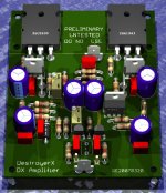
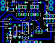
Greg , i had a look at your pcb, i like it 🙂
Much better than the one i had cooking in Eagle .
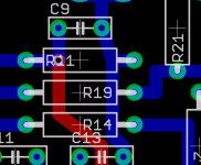
Regarding your two red traces:
I think with a bit of shifting of components, you can run the left one at the bottom of the pcb , where it is now.
I made a quick drawing for loosing the one on the right:
Reroute the connection from q1 to q3 as shown in black.
It would need a bit of shifting of components, but i think it could fit.
Graham , i agree with you on the optimal layout of the starground.
I just find it darn hard to implement on a pcb, maybe i'm just not smart enough
With kind regards,
Klaas
Much better than the one i had cooking in Eagle .
Regarding your two red traces:
I think with a bit of shifting of components, you can run the left one at the bottom of the pcb , where it is now.
I made a quick drawing for loosing the one on the right:
Reroute the connection from q1 to q3 as shown in black.
It would need a bit of shifting of components, but i think it could fit.
Graham , i agree with you on the optimal layout of the starground.
I just find it darn hard to implement on a pcb, maybe i'm just not smart enough
With kind regards,
Klaas
Re PCB
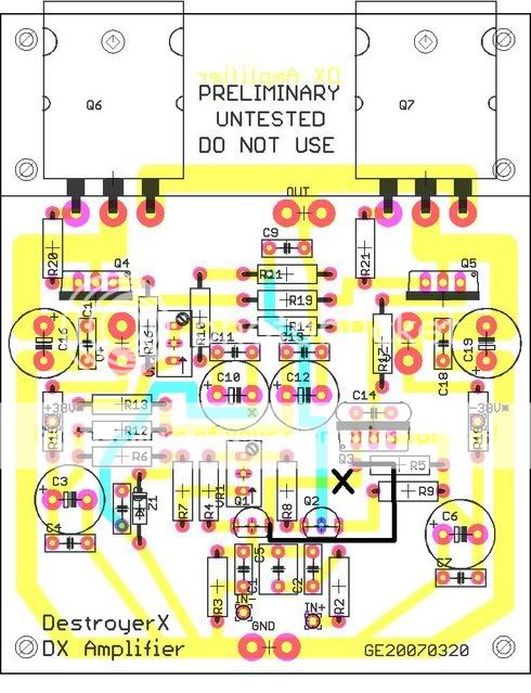
One R labelled R21 should be R11. The middle one ?
I cannot see the Zobel.
Cheers ........ Graham.
One R labelled R21 should be R11. The middle one ?
I cannot see the Zobel.
Cheers ........ Graham.
kvholio said:Greg , i had a look at your pcb, i like it 🙂
Much better than the one i had cooking in Eagle .
Regarding your two red traces:
I think with a bit of shifting of components, you can run the left one at the bottom of the pcb , where it is now.
I made a quick drawing for loosing the one on the right:
Reroute the connection from q1 to q3 as shown in black.
It would need a bit of shifting of components, but i think it could fit.
Hi kvholio,
Thanks for the suggestions. I have a little play around and see what happens. 😉
regards
Graham Maynard said:Re PCB
One R labelled R21 should be R11. The middle one ?
I cannot see the Zobel.
Cheers ........ Graham.
Hi Graham,
Thanks for having a look. There is a "temporary" via right behind the first "1" in "R11" which makes it look like a "2". I'm using back and forward annotation between the schematic and PCB so these kind of naming errors can't (shouldn't) occur. 😀
The intention is to have the zobel and output inductor offboard.
regards
Greg
Attachments
Lovely boards Greg..go ahead in your research.
I thank you very much for your cooperation.... every cooperation will be welcome.
Special thanks to Greg, that cooperate with me since the early beginning of this thread...you are free to decide things related the board Greg...but please, include some option in the board to help people to customize for their own needs....maybe a green and orange wires to travel under the board for the folks that wants the VBE multiplier.
If Klaas wants to make his version and to publish here, will receive my thanks...this way people will have more options.
Of course i am open to receive suggestions, and Roender suggestion was accepted...so Roender, no reasons to abandon us.
But the design was already made..some small changes were made...as optional diode biasing.... VBE multiplier using external board and some parts were removed.
But this is the end of modifications..for now on...to avoid too much confusion.
The working schematic was posted and soon we will have Greg finished board...maybe Klaas finished board too....i hope those friends can construct and test their boards to avoid future surprises.
Zobel was something Greg forgot and will be placed in place once again...also the optional holes to output coil will be there to keep people free to use it or not to used it.
The amplifier use low speed transistors as voltage and drivers, and this was done to be simple, and to be cheap..also to avoid surprises with oscilations in the HF bands...as those hi speed transistors are dangerous...their advantage is something that may not have too much advantages compared to the risks they provide.
The thread, in my point of view, gave the results i wanted... i could show the amplifiers, modifications were done, some contributions were accepted, a lot of hits shows that we had many visitors, Klaas had constructed and said sounds good...final board is arriving and my mission was finishing...
Everything that will happen here, in the future, will be much more than i hope for...maybe more people will construct, as pioneer Klaas have took the risks for himself...thanks Klaas....many folks may follow you in the future.
Final schematic published...final board arriving... amplifier already constructed by a forum friend...i am already happy and satisfied with that.
regards,
Carlos
.........................................................................................................
Nordic
I also think that separated supplies result in better channel separation (the best possible) and better sound stage.
regards,
Carlos
Hi Greg,
There is a nice spot between Q6 and the OUT terminations just waiting for the Zobel.
Just needs the earth and if a track is not possible then a single wire link might be better than two wires to an external Zobel.
Cheers ....... Graham.
There is a nice spot between Q6 and the OUT terminations just waiting for the Zobel.
Just needs the earth and if a track is not possible then a single wire link might be better than two wires to an external Zobel.
Cheers ....... Graham.
I wonder if I could make an observation here in relation to the Zobel capacitor.
I now choose a 250Vdc component for use with up to 60V rails.
In the past whilst 'messing about' I have either scorched or blown polyester Zobel capacitors. The point being that once the Zobel capacitor has failed internally and an amplifier has blown, simply replacing the odd blown transistor will not effect a repair and device failure is likely to be repeated. Some supposedly 'self heaing' capacitors might not show outward signs of failure.
Given that the 250V components do not cost much more, the risk of amplifier failure to a lesser component is a seriously false economy. The 250V ones tend to be slightly bigger though, and need increased lead spacing.
Cheers ........ Graham.
Thanks for the help Graham, I ripped all the earth wiring and did it over... made what I thought was an insignificant layout change, and what do you know, its working very nicely now....
Man !!!! these mosfets sound nice... Very Very smooth high frequencies, but at the same time super detailed...hard to believe it can sound that good comming through a cheap electrolytic, seems Carlos is right about that..
Man !!!! these mosfets sound nice... Very Very smooth high frequencies, but at the same time super detailed...hard to believe it can sound that good comming through a cheap electrolytic, seems Carlos is right about that..
Hi Nordic,
Good to hear of your problem being solved.
I'm a bipolar guy myself ( ! keep it clean ! ).
Anyone could have the best amplifier circuit in the world, yet it might sound rubbish if not laid out properly, or if a priority was placed upon making the pcb look pretty.
Thus a simple amplifier properly done is more than capable of surviving High Noon in Carlos-town.
Cheers ......... Graham.
Ok, still got a bit of drift after some listening, noticed biasing pots are running hot, could be due to proximity to the 2W resistor, or even through the solder joint to it... will try to thermally isolate it tommorow as well as throw a second transformer in to further seperaet the channels.. when it works it is lovely. Eats chips for breakfast.
Graham Maynard said:I'm a bipolar guy myself
Shocking.

I'm a closet type myself, never able to make up my mind and stick to either BJT or (take a pick)FET
Graham Maynard said:I wonder if I could make an observation here in relation to the Zobel capacitor.
I now choose a 250Vdc component for use with up to 60V rails.
Given that the 250V components do not cost much more, the risk of amplifier failure to a lesser component is a seriously false economy. The 250V ones tend to be slightly bigger though, and need increased lead spacing.
Cheers ........ Graham.
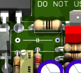
Hi Graham,
What is the size of the zobel cap?
On one amp I am building they use X2 caps for the zobel cap, 250VAC not DC rated. Size L19.5 x W8.5 x H14 15mm between leads. The attached picture shows it is a squeeze, so before I start moving all the components I thought I'd check I am using the right physical sized component.
regards
Attachments
kvholio said:Regarding your two red traces:
I think with a bit of shifting of components, you can run the left one at the bottom of the pcb , where it is now.
I made a quick drawing for loosing the one on the right:
Reroute the connection from q1 to q3 as shown in black.
It would need a bit of shifting of components, but i think it could fit.
Hi Klaas,
I took your advice and it worked out OK.
Thanks
Attachments
Greg, don't be so cheap, just make the board bigger!!!!!!! I stilll have to get a soldering iron in there you know... And I have seen carlos' stuff he solders with welding rods.... 😱 😀
My preference at this stage is basicaly for anything that works, lol.
I can make anything not work. getting a little better lateley as I put more dicipline into the work/layout.
A year ago I thought Carlos must be very smart, building all those many amps everyday... now I see, he is just as frustrated as I am. Else he would have stopped when it worked.
Morning uncle Charlie!!!!!!!!!
Its a public holiday here today, and the world does not seem so bad today.
- Status
- Not open for further replies.
- Home
- Amplifiers
- Solid State
- Destroyer x Amplifier...Dx amp...my amplifier