
Yup, my mistake above. Nixie62 is correct.I'm looking at the datasheet, it says H2 - Spdif and GND. Power supplies are on H1 ( H1.1 H1.2 for XMOS) and H3 ( H3.17 H3.19 for oscillators).
I used that. On those plastic DACs I left the SPDIF out so I could try it on the old DACs. Just need to configure JLS to have SPDIF output. I have the same with WaveIO board on DDDAC, Spdif output is also set there. It can sometimes be useful, when you already have it. One RCA or BNC to chassis.
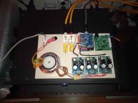
I have another occupation with JLS. I got a JLS stacked combo from a friend: I2S over USB, Oscillator board and AK4493 DAC board. It works fine, but it only has a USB input. Now I have to put the AK4118 SPDIF receiver board in it. The idea is to cut the I2S connection between the USB and the oscillator board, to go to the I2S input of the SPDIF board with MCLK, Data, BCK and LRCK, and then from the I2S output of the SPDIF board to return all those signals to the oscillator board, which forwards it to the DAC. Then there is a choice of input for USB or SPDIF/TOSLINK on the AK4118 board. And then it all goes back into the box with the tube gain stage (it was taken from there). 😁
Attachments
Last edited:
Wave I/O sounded better w/o the little smd transistor that allowed the SPIDF input....I used that. On those plastic DACs I left the SPDIF out so I could try it on the old DACs. Just need to configure JLS to have SPDIF output. I have the same with WaveIO board on DDDAC, Spdif output is also set there. It can sometimes be useful, when you already have it. One RCA or BNC to chassis.
I waited a cpld chip for my first V3 JLSounds to fix it after a short, but Luyben never sent it as I asked simple postal service w/o tracking (DHL and consors became expensive) to just purchase the cpld. Inside EC, VAT is expensive, a plain JLSOUNDS is 120 euros shipped to France. Which is odd as he provided support to debug the broked but fixable gear (which made me bougth the last V3 too before waiting a fix then to use for another DAC... ah that DAC disease we have)
Now I want slower crystal with 22/24speeed like the Wave I/O, an easy mclk output with matched ufl/smaimpedance output to avoid reflexion as much as possible, for reclocking and slaving whatever I want on the pcb before the dac inputs, etc. Better care of the front end make the DAC really sounds better as well. It had aalmost all : ufl outputs, non stop clock, 22/24 Mhz slower speed for our PCM chips... We have also @eclipsevl board with certainly better nowadays galvanic isolation chip I assume
Now I want slower crystal with 22/24speeed like the Wave I/O, an easy mclk output with matched ufl/smaimpedance output to avoid reflexion as much as possible, for reclocking and slaving whatever I want on the pcb before the dac inputs, etc. Better care of the front end make the DAC really sounds better as well. It had aalmost all : ufl outputs, non stop clock, 22/24 Mhz slower speed for our PCM chips... We have also @eclipsevl board with certainly better nowadays galvanic isolation chip I assume
Last edited:
I have to make it to work with what I have, otherwise I'd ditch the AK4493 and put in some Miro DAC. Unfortunately, there is no room or power supply for that. AK4493 has always been bass shy for me, I don't know why. I imagine the tubes will add some meat and fat, so that they are not just bones on the menu. 😁
Is it spdif output?Wave I/O sounded better w/o the little smd transistor that allowed the SPIDF input....
yes iirc, it was in the thread. Lucian removed it when you asked and using only USB. My reference DAC has it at the input then all UFL til sim mode up to TDA1541 chipp (2 cm from uf/l plugs) with in between Masterclock, isolation, reclocking and fifo and MCLK slaving of the logic for the sim mode. All flat, 50 ohms, no antennas, shielded (uf-l)
Last edited:
I came back to this thread looking for the gerbers to send another job to JLCPCB and I found a reference to this PCB on Miro's index (his link in post 1).cheers, diyiggy
Is a step file is ok enough for printing? Green is the two layers. Blue is the 4 layers with different digital streamer PS options.
Diyiggy, did you get to use this PCB? I am not sure if you intended to share you PCB design for others to use, but I see no straightforward way to go from that STEP file to Gerbers.
The post you refer to has a two layers for the communauty : there is a folder with the files in the post. It is exactly the one from Miro I worked on (the one with the JLSOUNDS header at the top) but two stages smd output and also 0805 pad for the 0.1 uF of the AD1862. It is an inverter input for a VFA then a buffer with a resistor in between and also a resistor to ground for the non inverting input of the I/V op amp. few basic improvments on the pcb. The voltage of the I/V syage + buffer is independant, the Analog voltage as the digital of the ad1862 are independants (the analog ones of the ad1862 where splitted for routing layout improvment). As the op amps have an independant PS, you can work with others voltages than 12, like 5V, 10V, 15V etc.
The 4 layers is going further to avoid current crossing of signals between them and also between PS themselves, all together with one other as well. Currents are "directed" and sometimes don't share so all the 4 layers according the areas, Some tht are not real THT to allow that where it is needed. It has more smd parts possible to setup the I/V (hence VFA as CFA are feasible + buffer with more precision. Most pads are 1206, but still some 0805. The layout is 100% mine with care to layers very small capacitance, 50 ohms touting, care of the digital lines signal integrity. Alas some choices has to be made because high speed nowadays op amps, so no THT parts but the output resistor where I favor for my own taste more carbon comp or carbon film. Dale RN60 or Yageo 0.1% metal are okay if some want metal. the size is circa 9x8 cm, you must have the JLSounds USB side feeded (no header there), the digital side can be feeded from the 5V of the AD1862 digital or can be splitted. In both case the digital lines will stay quiet for the upper AD1862A unit. uf-l are at the bottom for some reason, to allow even better routing. needs your on logic before or I2StoPCM from IanCanada that needs itselfs to be MCLK feeded and I2S feeded (Wave I/O for instance has the I2S + MCL uf-l output).
if some wants the 4 layers, could be a GB at democratic price just to cover the hassle of posting plus yummy coffee if someone is making a GB interet list in the Diyaudio GB. JLPCPCB is per 5 units to make a batch. I don't want to release it free with gerbers to feed the chineese or whatever country kitchen market as I think it is better than all what I saw in commercial gears, be it DIY too. Maybe I'm biased. I don't ptopose it because it is for my needs and I think most want free stuffs and not almost free stuffs ! 🤔
Last edited:
Hi diyiggy, I tried when I saw it, but it does not work, it needs to be a zip with the Gerbers I believe.
Let m try this week to fix the problem. It is a JLCPCB made package from Kickad 8, at least it should.
It was downloaded more than 70 times, maybe noone used it, dunno !
It was downloaded more than 70 times, maybe noone used it, dunno !
My best Mariah Carey for all to Christmass.
Swak,
I sligthy enhanced it the last hour. It replaces the Step file here Old Step file that is a mess for Gerber files packaged for JLCPCB linked here (@miro1360 if you may edit this link by this post for your Blogspot acuracy 🙂 ) !
So it is the Miro's pcb for ad1862, 2 layers with headers for stacking JLCPCB V3 and uf-l inputs I asked long time ago at the beginning of this thread. I have changed nothing from this front-end side of the pcb. Miro1360 sended me some files to help on it. We can thanks him again & again!
Decoupling resistor to the non inverted input to gnd of the I/V op amp had been added. Put a zero ohms if not needed.
Feedback cap & resitor must be soldered on their sides the foot print is 1210 size, confortable : I made the pads bigger than the previous. Non inverter input R or jumper to GND is 0805 footprint.
Decoupling power caps are 0805 : COG/NPO or 0.1 uF acrylic (CDE). resistor at the output of the I/V op amp is 1208 footprint (soldering on the side of the resistor advised too for good practice).
J3/4/7/8 and -VDC must be populated at the bottom side.
Two op amps are inverted input pin topology.
I have been uploaded it on JLCPCB : 7 euros ! share with peeps if you have pcb left ! 🙂
If some interrested by the 4 layers pcb here for a very small cost (less than a bad TDA1541A's pcb design sold elswhere, lol), let me know or organise a GB interrest list on the dedicated area of the forum. Diyiggy's AD1862 V3 - 4 layers.
Attachments
Last edited:
It has independant op amp power supply header so you can try whatever VFA op amps you want at the voltage you want. The secondd op amp buffer can be handy to help the I/V according the op amp you choose. You can make as well a very good headphone driver by choosing a strong buffer if you need or to simply drive loads with ease if you need.
The two PS headers for the AD1862 analog side 12V belongs to the same reg output. So Miro's 1360 regs can be used if you want (you just need one more for the +5V digital, but it can be took from the double V outputs pcbs from Miro as well. At the end it is still a star ground big pcb with separate AGND/DGND populated areas (so ADGND ground if you prefer 🙂 ).
The two PS headers for the AD1862 analog side 12V belongs to the same reg output. So Miro's 1360 regs can be used if you want (you just need one more for the +5V digital, but it can be took from the double V outputs pcbs from Miro as well. At the end it is still a star ground big pcb with separate AGND/DGND populated areas (so ADGND ground if you prefer 🙂 ).
Last edited:
Hi Iggy,
Thanks for sharing your spin on AD1862 MiroDac 😉.
Did you post a matching schematic somewhere in the thread?
Thanks for sharing your spin on AD1862 MiroDac 😉.
Did you post a matching schematic somewhere in the thread?
Nope. The 2 layers gerber:
Classic inverted pin input. Non inverted to ground(resitor or direct). Output resistor then non inverting input for buffer or more gain. Up to you to size the passive parts according the vfa op amps. The cap between the op amps arts both as output and next stage input resistor.
It stays NOS.
Classic inverted pin input. Non inverted to ground(resitor or direct). Output resistor then non inverting input for buffer or more gain. Up to you to size the passive parts according the vfa op amps. The cap between the op amps arts both as output and next stage input resistor.
It stays NOS.
Last edited:
- Home
- Source & Line
- Digital Line Level
- DAC AD1862: Almost THT, I2S input, NOS, R-2R