
I advice you not the D3 road, but more an inexpensive miro1360, just to have an idea of the chip sound.
If you want something more concistant, wait the other thread or go the GB of audialonline AYA5 . TDA1541A is more complicated than many of the other pcm chips....
If you want something more concistant, wait the other thread or go the GB of audialonline AYA5 . TDA1541A is more complicated than many of the other pcm chips....
"DM" is something I picked up from my teenage daughter. Diligent Mail, seems like a good interpretation 😊 In any event, I sent Vunce a message re the board.
I was planning to try the chip in Miro's board. As you suggested, it seems like an easy approach to get an idea of the sound and how it compares to the AD1862 and PCM63 in a very similar context.
Happy Sunday.
I was planning to try the chip in Miro's board. As you suggested, it seems like an easy approach to get an idea of the sound and how it compares to the AD1862 and PCM63 in a very similar context.
Happy Sunday.
I can confirm that this PCB works and does so really well! 🙂 I finished soldering it this morning and hooked it up to TDA1541A (it was on the bench and easiest to test with). Not sure if I need to change anything for TDA1541A (old D3 build), but sounds good to my ears!I/V based on TPA6120
edited post #9463 (added R3, R4 on the output signal, hole in the GND under the feedback trace)
Power supply range is from +-5V up to +-15V. It can be powered directly from DAC PSU.
R1 and R2 value determines the output voltage. For a higher output voltage use higher value of this resistor (1k5 == 1.5Vp, 2k7 == 2.7Vp, ...).
R3 and R4 resistors melf 0204 or SMD1206, value 22R up to 100R.
Capacitors are polypropylene and a high quality electrolytics (UKW from Nichicon is still available).
There is hole in thermal pad under the IC, where you solder the IC with PCB from the bottom.
IL, IR is current input from DAC.
VL, VR is voltage output.
Note, that a small (not harmful) DC offset may be present in the voltage output.
This is redesigned PCB and so far not tested.
BOM example: https://mouser.com/ProjectManager/ProjectDetail.aspx?AccessID=5ca5f6fb0b
If what you want is +/-5V x2 then simply populate the 2nd set of regulators for 5v instead of 9v.@miro1360
Is it possible to make the PSU2 board output dual 5v instead of 5v+9v? I want to use it to power the I2soverUSB board.
If so what do I have to do.
Without having schematics in front of me. This would be done by populating the 2nd pair of regulators with the same value resistors and caps as the 5v pair.
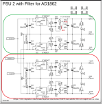
Yes, this way you will get positive/negative 5 volts on both sidesThanks for your reply.
So basically I have to replace the bottom portion of the schematics (RED) with the top half (Green) as per the attached schematics? Ie. copy paste?
Not from the same PSU2 board to externally power the JLS board.
The JLS board needs its own separate 5V/GND, 5V/GND supplies to remain isolated.
The JLS board needs its own separate 5V/GND, 5V/GND supplies to remain isolated.
If that is the case, the suggestion by Vunce is the most practical solution. Prepare one 5V for the 'dirty side' and another 5V for the reclock and clock, which is the 'clean side' of the JLSOUNDS board. The isolation is important here, or you will waste the potential of the JLSOUNDS performance.
Just a recommendation:
https://a.aliexpress.com/_ooEGhEz
Get two of these.
Or use the Gerbers from Miro for the LT1963 mini. Use two individual ones.
https://www.diyaudio.com/community/...s-input-nos-r-2r.354078/page-439#post-7739220
Just a recommendation:
https://a.aliexpress.com/_ooEGhEz
Get two of these.
Or use the Gerbers from Miro for the LT1963 mini. Use two individual ones.
https://www.diyaudio.com/community/...s-input-nos-r-2r.354078/page-439#post-7739220
I did share +5v for jls clean side and +5v from usb cable(pc side)Not from the same PSU2 board to externally power the JLS board.
The JLS board needs its own separate 5V/GND, 5V/GND supplies to remain isolated.
Eventually I had another regulator for jls clean side.
How many transformers do you guys use for 1 project?
Dac < PSU2 feeding 5v and 12v < 2x transformer (12-0-12v 1.5a 35VA) Should i reduce it to 1x transformer?
Tube IV (by grunfs and michealag) < PSU 1x transformer (170v 0.13A 6.3V 5A 53.6VA)
I2SoverUSB < 2x PSU (15Euro from JLsounds) feeding 5v and 4v to the board (according to Lyuben from JLsounds) 1x transformer (Triad Magnetics VPT18-1390 Parallel 9.0VAC 2.78A 25 VA)
The transformers for the DAC and IV will be custom wounded by a local supplier in Thailand.
It seems that I'll be needing a lot of space. Is this overkill?
One transformer for PSU2 (0-12v 0-12v secondary)
I prefer Rcore.
One transformer for +5v JLS clean side.
Better quality regulator preferred.
You can add another PSU transformer+reg for dirty side.Those transformer must be separated.
And another one for tube IV
I prefer Rcore.
One transformer for +5v JLS clean side.
Better quality regulator preferred.
You can add another PSU transformer+reg for dirty side.Those transformer must be separated.
And another one for tube IV
It depends on the complexity of the device. I practice one transformer for the digital part, with several secondaries (3-4 sec.) of 8VAC for JLS-XMOS +5V, JLS-Oscillators +5V, SPDIF board +5V, digital part DAC +5V and digital part DAC -5V. I steal the +5V connection for the mute circuit from one secondary. The second transformer has two 12VAC secondaries for the +-5 and -+12V analog part of the DAC. Sometimes that second transformer has also two secondaries at 8VAC for the analog part of the DAC +-5V if I'm not using PSU2. I manage depending on the configuration. PCM56 and AD1862 have a +-12V power supply for the analog part and opamps, so one +-5V power supply is redundant. This last small DAC with AD1862+Amanero USB has only one transformer 20VA (on core 30VA) with 2x12V for DAC and 1X9V for display. The transformers are custom made here locally, according to my wishes. Static shield, magnetic shield, winding on a larger core with reduced magnetization, defined lead position to fit nicely and the like.How many transformers do you guys use for 1 project?
You should take into account the required currents of each secondary, the required AC current is 1.41xDC current. It is of course the minimum of the minimum, it is good to oversize it several times. The more the better. One of the reasons is that in the transformer - diode bridge - capacitor schematics, the secondary current is not sinusoidal, but a series of strong pulses (100Hz or 120Hz) to charge the capacitor. That's why you should always oversize the secondary and diode bridge. Mains transformers are normally dimensioned for sinusoidal current, not impulse current.
PS
I use PSUD2 free software for the simulation, the schematics is set there and then all the events can be seen nicely. You just need to enter the correct measured data for the transformer and capacitors (voltage and DC resistance of secondary, capacitance and ESR for capacitors).
Last edited:
And another one for tube IV
If You consider clean and dirty sides than Tube I/V must have separate transformers for high voltage and another for heathers - that is the oldest "proper" way ( mainly relevant at amplifier level, but useful anyway ).
- Home
- Source & Line
- Digital Line Level
- DAC AD1862: Almost THT, I2S input, NOS, R-2R