You can buy Y instead of BTC. Their prices grow similarly. 🤣Come to think of it, we should all have made the first one with AD1862 so we don't waste money on the rest.
Someone here knew what he was doing as soon as AD811 was there (but again there is a small error in the circuit), AD843 is a great op amp but also expensive and a filter is made around it which can be avoided if a filter is inserted into the IV stage with AD811 like in mine version.
Now there is again a debate whether a filter is necessary, my opinion is Yes. In my case, the cutoff is only around 40kHz, which is enough to prevent any HF noise that can come out of the DAC.
Now there is again a debate whether a filter is necessary, my opinion is Yes. In my case, the cutoff is only around 40kHz, which is enough to prevent any HF noise that can come out of the DAC.

Where is the error in the AD811 circuit?Кто-то здесь знал, что делал, как только появился AD811 (но опять же небольшая ошибка в схеме), AD843 отличный ОУ, но тоже дорогой и вокруг него сделан фильтр, которого можно избежать, если фильтр вставлен в IV ступень с AD811 как в моей версии .
Сейчас снова идут споры, нужен ли фильтр, мое мнение – Да. В моем случае частота среза составляет всего около 40 кГц, чего достаточно, чтобы предотвратить появление ВЧ-шума, исходящего из ЦАП.
After a lot of delay my DAC is alive !
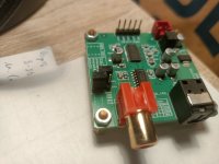
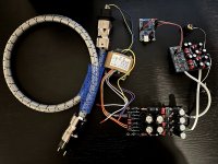
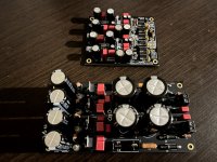
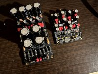
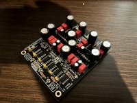
PCM1702 + Hybrid ECC86/mosfet I/V
I received the chip and it was functional .. @NIXIE62 you were right about running the Hybrid I/V without iv resistor . The gain is spot on without a resistor . Easily drives preamp or HPA now . I will test it with my Aikido preamp + F4 later .
I still have some cable arrangement to do but i have been listening with my Noir HPA for 2 days now and i have a happy face 🙂
I am really impressed with the sound .. rich with clarity , bass so full , middle clear and precise , nice highs .. no fatigue .. just a warmness of sound.
Thank you @miro1360 for your work you gave to the DIY Community and thanks to all the nice people here assisting .
Attachments

Last edited:
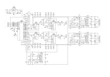
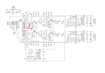
As mentioned here I completed my AD1862 DAC with Pedja Rogics discrete diamond non feedback IV:
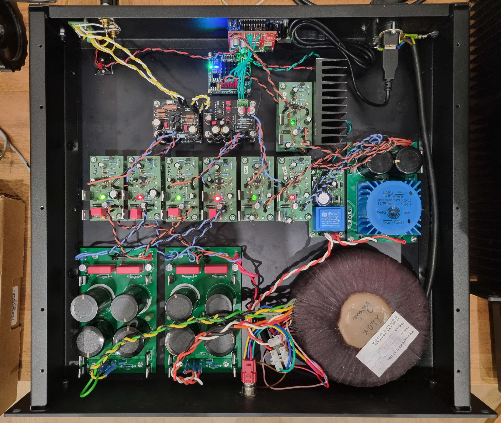
It's not easy visible on the picture, but it's built in 2 layers as dual mono: one channel is on the lower level of PCBs, the other channel is upstairs. There are 14 super regulators (ALWSR), the 16x interpolation filter by Kusy Audio, separate transformers for analog (large toroid) and digital (blue Talema). The small blue square transformer feeds a housekeeping PCB that controls the mute relay which sits next to the RCA outputs. The sound is very good.
My question is: I now use 3K7 as the IV resistor at the end of the diamond buffer to get a normal output voltage, but iirc lower values will result in less distortion - is that the case even if the DAC chip doesn't drive the IV resistor directly?
Last edited:
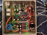
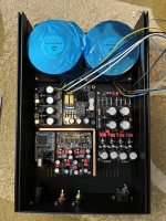
My work in progress so far ... I started with a normal USB-powered I2S board configuration, but then I decided to use a separate PSU. Due to some limitations, It would not be possible to use a normal Modushop stainless steel base plate, I will have to find another way. I am still waiting for Burson audio OPAMP. Hope I will finish it next week.
Attachments
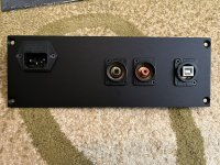


It all looks very nice. I have only one remark, about the USB connector on the chassis. You have that connector, then a piece of USB cable with two connectors, and then the connector on the JLS card. Since USB cables and connectors affect the final sound, we practice to have the JLS card directly against the back panel and only have an opening to attach an external cable to the board connector. Additional connectors and cables are not recommended.
I agree. But how long does it take until the USB connector breaks from the small PCB? It's just a question of time. Some day sooner or later it will happen.
Alea iacta est ... I won't be able to change this layout, since the back panel is fully customized to this specific solution. The reason why I decided to do this is only pragmatic. It should provide easier assembly and also sturdiness. Maybe if I was able to find the socket component with the same size as NEUTRIK connectors and USB connectors, but without inner filament, in that case it would be possible. It could be also possible to maybe print 3D model for it. The printed socket would attach tightly to the USB connector on the board and also have outer dimensions as the current USB connector socket. However, I am not planning to drill any additional holes or modify the back panel.
It depends on the usage. I have been using the WaveIO USB/I2S card for over 8 years, the connector on the PCB is still in perfect condition. It can happen of course with some very rigid DIY cable that the connector is mechanically damaged. Yesterday I replaced one on a JLS board, which was damaged by a DIY USB cable. It's not that difficult, because I have a desoldering station with a vacuum pump. Otherwise it can be painful. PCB itself is bullet proof, really strong.
Last edited:

Well, it's solidly big. I think I already mentioned here, reduce the supply voltage for the XMOS part to 4V. Then a smaller cooler is sufficient.Another limitation on the JLS board is caused by me. I mounted a heatsink, since with the previous one, it got pretty hot.
I don't think the BD139 will just burn out even with the original cooler, but I really don't like any component to heat up that much.
Last edited:
Give us a schematic please. I/V has to exist somewhere (active or passive I/V), the DAC chip is with Iout. I don't remember exactly what I told you. 🤔I received the chip and it was functional .. @NIXIE62 you were right about running the Hybrid I/V without iv resistor . The gain is spot on without a resistor
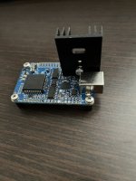
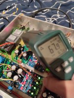
I observed that one of the transformers is getting hot after a while . i can barely touch with my finger . it reaches almost 70°C . It's an Indel 6V 1.16A that is feeding LT3042 regulator 3.3V for CM6631A usb i2s board . consumption of CM6631A according to datasheet is only 80ma . What is wrong? perhaps defective transformer ?
Attachments
- Home
- Source & Line
- Digital Line Level
- DAC AD1862: Almost THT, I2S input, NOS, R-2R