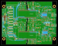
Here's how I did it Tamra. You have to ignore the silkscreen. The u.fl follow through to the header underneath. All the u.fl have a ground from the Fifo so you dont need to do it like this if it is better to just use one. I've had no issues with this though.
Attachments
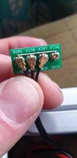

If the I2S wires can be soldered from the bottom of the black PCB, maybe those connectors can be avoided?
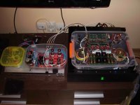
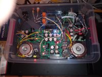
I am slowly putting together a Miro DAC prototype.😎 In fact it will serve to test three Miro DACs. First AD1865, then PCM63/PCM1702 with adapter and finally PCM56/AD1856/AD1860. The inputs will be USB, SPDIF and TOSLINK. The power supplies were made with LT1963/3015 off-the-shelf modules from ebay on raster boards. A slightly different active I/V circuit is planned for later. For that I/V I planned a more powerful +-12V power supply (the one with a large cooler). I don't have much time due to increased business obligations, otherwise this would have been over a long time ago.🙄
Attachments

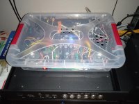
I really like the plastic container chassis. It gives me some ideas since my Miro DACs just sit on wooden boards.
My lazy *** has still got pcm63 like that, wooden board and catching dust like crazy xDI really like the plastic container chassis. It gives me some ideas since my Miro DACs just sit on wooden boards.
Last edited:

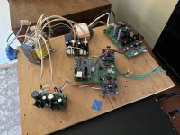
I used the holidays to get this up and running. I finally have a working Miro DAC.
To begin with, I inserted the Miro AD1865 board, and then the rest will go one by one. When I find some time.
Aliexpress/ebay power supplies with LT1963/3015 work flawlessly. They are mistreated with resistors well before connection.
DAC has all popular inputs, USB, SPDIFx2 and TOSLINK. In addition to the analog outputs, it will also get one SPDIF output from the JLS board for the weekend.
For now, I have no objections.
The OPAs are Burson V5 at the moment.
There is no remote control. 🤣
Attachments
Last edited:
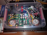
The DAC is a bit messy, unfortunately it's a small box and barely everything fits, there are too many wires and connectors. Since this is a test sample in which various DAC chips will be tried, this is how it had to be.
The final version will be in a bigger box and a better optimized layout, and I will replace many connectors with direct soldering.
In the meantime, I tried two more OPAs for I/V, the Burson V6 Classic and the OPA1611. I can say that this Burson V5 is by far the best match with the AD1865. Since it's an old model, Burson V6 Vivid and Sparkos SS3601 are probably suitable for similar sounding new models.
Tried last night Kiwame carbon film resistors 2k7 1W for I/V. Something is better and something is worse than with DALE metal film. With DALE the sound is drier and tighter, with Kiwame it is warmer and the sound is more fluid, however the bass with Kiwame is too soft, so it remains DALE for now.
I have both DALE and Kiwame 1k5 to try with PCM63, so I'll see how that goes. The PCM63 has proven to be sonically brighter than the AD1865 in several devices so far, it might be fine with the Kiwame.
To my surprise, the AD1865 can work cleanly in this configuration with a 24bit 384kHz PCM signal.
I have both DALE and Kiwame 1k5 to try with PCM63, so I'll see how that goes. The PCM63 has proven to be sonically brighter than the AD1865 in several devices so far, it might be fine with the Kiwame.
To my surprise, the AD1865 can work cleanly in this configuration with a 24bit 384kHz PCM signal.
PCM63 inserted (finally). Burson V6 Classic is the best match for PCM63. With the Burson V5, the treble dominates and the bass is somewhat hidden. With the V6C, everything is in its place.
I'm waiting for the AD1860 to arrive, to assemble that PCB and give it a try. I know it won't be better than the PCM63, but I'm curious how it sounds compared to the AD1865.
I'm waiting for the AD1860 to arrive, to assemble that PCB and give it a try. I know it won't be better than the PCM63, but I'm curious how it sounds compared to the AD1865.
Attachments
There is one small thing. On the I2S connector on the PCM63 board (pins 2,4,6 and 8) pin 8 says GND, but it is not connected to GND. I connected that from the bottom (pins 7 and 8) so as not to change the connector I used for the AD1865. I have no idea why it is not connected to GND and it says GND? I didn't notice before. This is important to me because the AK4113 and the JLS output part are grounded through that pin to DAC GND.
Attachments
I have another question, with some OPA I have a solid DC offset at the output. With Burson V5 it is about +9mV and with Burson V6 C it is about +25mV. Is there a way to correct this? Not on this PCB because there is no room there, but if I make a separate I/O with OPA.
- Home
- Source & Line
- Digital Line Level
- DAC AD1862: Almost THT, I2S input, NOS, R-2R