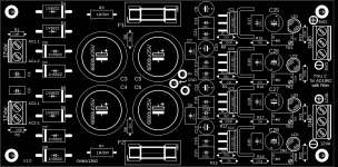
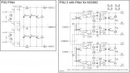
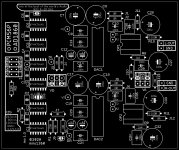
PSU 2 not only for AD1862
PSU 2 is based on LT1963A/LT3015 LDO regulators.
Why I chose these regulators? Letting DIY people only on 78/79 regulators would not be fair, so I was searching and found an inspiration in this test:
A-comparative-overview-of-power-supply-regulator-designs-with-listening-tests
In the basic configuration, components are set to output the +/-5VD and +/-12VA for AD1862 DAC.
These regulators are adjustable and are set via resistors and fine tuned using a trimmer.
Again, the output power and heatsink is a DIY question, but since the AD1862 DAC consumption is small, it should go without heatsink
PCB size is 75x150mm and is universal - you can solder components for any other DAC voltages.
It can be cheaply ordered from jlcpcb or any other PCB manufacturer.
(it was not tested at the time of writing this post)
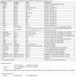
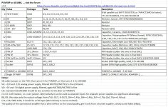
Example list of components (copied from BOM picture, except resistors)
mouser:
603-FMP300FRF73-1R
505-MKP20.01/400/5
R79IC3100Z340J, 505-MKP2D031001FJO00
667-EEU-FR1E101
667-EEU-FR1V271L
647-LKG1V682MESYAK
72-T93YB-2K
72-T93YB-100K, 594-64Y503
72-T93YB-100K
72-T93YB-200K
604-L483GDT
511-1N5822
863-1N4007G
584-LT1963AET#PBF
584-LT3015ET#PBF
534-4628
576-0216001.MXR20SPP
651-1729128
651-1729131
ebay: 233823483402, 233670142926
PSU 2 is based on LT1963A/LT3015 LDO regulators.
Why I chose these regulators? Letting DIY people only on 78/79 regulators would not be fair, so I was searching and found an inspiration in this test:
A-comparative-overview-of-power-supply-regulator-designs-with-listening-tests
In the basic configuration, components are set to output the +/-5VD and +/-12VA for AD1862 DAC.
These regulators are adjustable and are set via resistors and fine tuned using a trimmer.
Again, the output power and heatsink is a DIY question, but since the AD1862 DAC consumption is small, it should go without heatsink
PCB size is 75x150mm and is universal - you can solder components for any other DAC voltages.
It can be cheaply ordered from jlcpcb or any other PCB manufacturer.
(it was not tested at the time of writing this post)
Example list of components (copied from BOM picture, except resistors)
mouser:
603-FMP300FRF73-1R
505-MKP20.01/400/5
R79IC3100Z340J, 505-MKP2D031001FJO00
667-EEU-FR1E101
667-EEU-FR1V271L
647-LKG1V682MESYAK
72-T93YB-2K
72-T93YB-100K, 594-64Y503
72-T93YB-100K
72-T93YB-200K
604-L483GDT
511-1N5822
863-1N4007G
584-LT1963AET#PBF
584-LT3015ET#PBF
534-4628
576-0216001.MXR20SPP
651-1729128
651-1729131
ebay: 233823483402, 233670142926
Attachments
-
diyAudio_Stabilized2-with-Filter_for_AD1862_2021-02-11.zip464.5 KB · Views: 520
-
 diyAudio_Stabilized2-with-Filter_for_AD1862_PartsView.jpg403.1 KB · Views: 1,908
 -
 diyAudio_Stabilized2-with-Filter_for_AD1862_View.jpg279.9 KB · Views: 1,996
 -
 diyAudio_Stabilized2-with-Filter_for_AD1862_Schematic.jpg559.8 KB · Views: 2,051
 -
 diyAudio_Stabilized2-with-Filter_for_AD1862_BOM.jpg454.5 KB · Views: 2,114

Wow! You are a very busy man, Miro!!
So many options in this thread to build a great NOS R2R Dac. Now more PSU choices, nice job 😉
So many options in this thread to build a great NOS R2R Dac. Now more PSU choices, nice job 😉
DG,
You need a fifth set of speakers....
Don’t forget about the FAST TL’s
But, you might need another bottle of adult beverage for that one, Hehe!!

I was sure you guys would see more the bottle than the little ScanSpeak near it 😀
The bottle is for the study of the soul vibration behavior of the designer ! I resonate after a 25 cl load of 14 yo Spey W. ... hey !
 .
.But the dac is listened on a serious Loudspeaker designed by the great Phil Jones...
@Miro : that's a serious reg : )
Darlington reg with no feedback at its output while technically being inferior than with one on the output is sounding very good and better than with feedback (Tip 146 for example).
Nazaar fellow in a blog here made a good sounding & fast for the analog with few parts and very cheap as well. But for the noise of it, these modern chips are hard to beat...
While because of the layout around I see the TS7A Ti reg chips give better result for my ears than the LT30xx we often see on a little board with the 75/79xx 3 pins reg arrangement.
Last edited:
Hello!
I have Ian Canada LiFePo PSU and use to RPi, FiFo and ESS DAC, but I want to try with AD1862 so I thought that I like to use the batteries also to AD1862.
The rail from LiFePo is only +5V and 3,3V, so I want use only to charge the batteries.
I'm not proffessional but I thought it would be better if an OPA help the symmetrical rail.
In TINA software shows that it can be works but in practice I don't know. It's operably? What is your opinions this plan?
Hello,
Do the TL431 ref not need some cap filtering ? Something like a 1000 uF + a little film cap // ?
Notice I'm not specialist either...
Do the TL431 ref not need some cap filtering ? Something like a 1000 uF + a little film cap // ?
Notice I'm not specialist either...
@topicreader
virtual ground formed via opamp is not the best option due to a higher current consumption by DAC which not each opamp can handle (you could consider a chip amplifier or very good opamp which can handle high current, see this https://www.edn.com/simple-ps-voltage-splitters-based-on-audio-amplifiers-part-3/ ) ...
use more batteries and filter the output with some LDO regulators (you can use some cheap regulators or LT1963A+LT3015) .. or for the simplicity go with MC78/79xx regulators
if more batteries are impossible, go with 2x boost-buck DC-DC converters (one for +-8V and the second +-15V) and clean the output with regulators (+-5V +-12V) ... look ebay item: 202492860017
Last edited:
I'm thinking of modifying the board for direct I2s input from the jlsounds I2S over USB board, without the shift registers as described by Miro here. So a modified board without the shift registers and added traces/pads for the connections.
1) would that be ok, I don't want to offend anyone by doing so.
2) is there any down side to this other then losing flexibility in choosing usb to I2s boards?
1) would that be ok, I don't want to offend anyone by doing so.
2) is there any down side to this other then losing flexibility in choosing usb to I2s boards?
Last edited:
I'm thinking of modifying the board for direct I2s input from the jlsounds I2S over USB board, without the shift registers as described by Miro here. So a modified board without the shift registers and added traces/pads for the connections.
1) would that be ok, I don't want to offend anyone by doing so.
2) is there any down side to this other then losing flexibility in choosing usb to I2s boards?
Like this?
https://www.diyaudio.com/forums/dig...862-tht-i2s-input-nos-2r-138.html#post6492735
I made an error with those PCBs but have some replacements on the way.
Ordered boards and 1862s tonight. It is a project for the future months as I finish out some other tasks.
Damn, I thought I read through everything... But yeah, like that 😱
The replacement PCBs will be arriving soon (I hope!) so let me check them and maybe we can sort out a pair for you. BTW, in case you hadn't noticed, there's no I/V stage on my PCBs as I plan to use tube-based I/V.
The replacement PCBs will be arriving soon (I hope!) so let me check them and maybe we can sort out a pair for you. BTW, in case you hadn't noticed, there's no I/V stage on my PCBs as I plan to use tube-based I/V.
If you have a second pair, I'd gladly take them off your hands.....
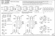
PCM56P, AD1860 ... 1 PCB for 6+ DACs
User @mllum asked for an universal layout for a few different pin-compatible DACs, #1443
PCM56P: 16-Bit; +-5VD, +-12VA (or +-5VA)
AD1860: 18-Bit; +-5VD, +-12VA (or +-5VA)
AD1851: 16-Bit; +5VD, +-5VA
AD1861: 18-Bit; +5VD, +-5VA
AD1856: 16-Bit; +-5VD, +-12VA (or +-5VA)
PCM61P: 18-Bit; +-5VD, +-12VA (or +-5VA)
... maybe another pin-compatible DAC exists
... SB solder jumper on the PCB select between bits, example:
- Short pins 2-3 for PCM56P (16-Bit)
- Short pins 1-2 for AD1860 (18-Bit)
These DAC chips can be considered as a lower cost solution (as they still be cheap). It may surprise with the sound as there are enough of them to test 😎
I don't know much about the sound from these chips, there may or may not be an audible glitch (according to the datasheet it should be neglitible).
Each DAC has 3 pins taked out on the PCB for optional MSB adjustment (-V1, A1, T1, -V2, A2, T2). The adjustment consists of 3 hand-wired parts in series (resistor-trimmer-resistor). This procedure is not very simple, hence optional.
>>...pcb for 8 dac ic's 4 for the left channel and 4 for the right channel
This is not achieved in my PCB due to overall complexity. DAC chips can't be paralleled without decoupling and filtering capacitors. Doing this for 8 chips would significantly enlarge the PCB. Moreover this DAC is not tested if it even works 😀 Check it for possible errors before ordering.
Some people have made parallel chip-to-chip connections, where some pins left unconnected (4, 9, 10, 11, 14, 15) and power pins were decoupled for each chip and connected together underneath - right on the PCB (in this solution a higher digital interference can be present).
Alternatively the 4 same PCBs can be assembled, one with digital glue logic an 3 without glue logic, and all PCBs without opamps - just DACs with capacitors). The first PCB with assembled logic will drive the other three in parallel (BCK, DR, DL, LRCK, GND). The Iouts will be linked together for each channel (here one PCB can act with I/V opamps (R8,R9 value is 1/4 of the value from single DAC) or a passive I/V resistor ... or another I/V solution). Note, that only Iouts shall be linked parallel, not Vouts.
Example list of components (copied from BOM, except some resistors)
mouser:
771-HCT164D652
594-SFR25000Z0000ZA5
C320C104K1R5TA
R79IC3100Z340J
667-EEU-FR1E470
UFG1C471MPM
80-C1206C470G5G
538-87914-0804
575-343308
575-1154731641003000
Attachments
-
 PCM56P_AD1860_PCB_TopView.jpg231.3 KB · Views: 1,210
 -
 PCM56P_AD1860_PCB_PartsView.jpg254.4 KB · Views: 1,355
 -
 PCM56P_AD1860_PCB_Schematic.jpg832.2 KB · Views: 1,422
 -
diyAudio_PCM56P_AD1860_DAC_BOM.zip10.4 KB · Views: 323
-
diyAudio_PCM56P_AD1860_DAC_gerbers_2021-02-14.zip613.5 KB · Views: 317
-
 PCM56P_AD1860_PCB_BOM.jpg425.1 KB · Views: 1,322
As far I'm concerned, in this list, only the PCM56P and its little brother worth it, been there already ! But why bother, if you have a tda1541 (crown or late South Asia made) and AD1862, why loosing your tie elswhere for less good ?
USB to I2S have all not the same order of Clk, Lrck & Data and Gnd... on dac pcbs and it's a lot of pain.
it's easier if through hole to make larger spacing on a dac board between the vias and to add gnd vias between each I2S via... or the uf-l pads... but here only the Rpi hat, the Wave I/O and IanCanada stuffs have some advance and also respect the 50 ohms impedance between the boards.
A stack à la Nautiboy is the way to go if the impedance spacing is ok in the layout design... it also means one board design per I2S board brand (JLSound, Wave I/O, Amareno, I2S Chineese Fi, etc as all have different spacing...
When here I asked to add uf-l pads on the 2014 AYA DAC years ago, it had a lot of sucess just because, the impedance matching and the compatibility with IanCanada stuffs which used to be the best source before. Just too bad than 2" uf-l cable are difficult to source or too much expensive... but 4" is ok.
Last edited:
"As far I'm concerned, in this list, only the PCM56P and its little brother worth it, been there already ! But why bother, if you have a tda1541 (crown or late South Asia made) and AD1862, why loosing your tie elswhere for less good ?"
There was a time, when Kondo then still called Audionote put out a commercial DAC for sale which I believe had 32 pieces of PCM56 dacs with 16 pieces of PCM56 dacs per channel.
I have never heard it, but Kondo's approach must have had some merit, if he put it out for sale; given their reputation in Japan and around the world as purveyors of some of the most expensive and high end audio equipment.
- Home
- Source & Line
- Digital Line Level
- DAC AD1862: Almost THT, I2S input, NOS, R-2R