
@Baobei great stuff, very tidy build. I have the exact same chips, those ones are made in USA apparently hence the different markings. Got some more on the way, hopefully the same USA made.
You could test powering the USB module from the existing 5V rail to see if it is worth it. You will need a 3k3 - 4k7 pull down resistor on the DAC board for the USB H1 connector.
You could test powering the USB module from the existing 5V rail to see if it is worth it. You will need a 3k3 - 4k7 pull down resistor on the DAC board for the USB H1 connector.
Congrats, very nice build! I bet it sounds great!Well, I took the plunge and bought a pair. I was slightly worried as the markings looked different (see picture). They do seem to work just fine though (listening to them now)!
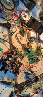
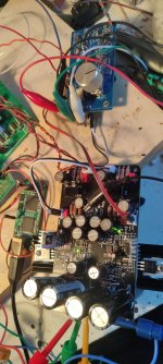
Using the PSU 1 Eco so the PCBs stack because I wanted a compact build for my desk. Sounds fantastic with my Whammy HPA and ACA Mini. Turns out there is actually still a bit of space in the case, so I'm contemplating squeezing in another transformer and a PSU2-Mini to power the USB-Board.... Wondering if it would be worth it.
I recommend to review this article for grounding best practices https://www.diyaudio.com/community/threads/audio-component-grounding-and-interconnection.163575/
Hi, I am new to this thread, but I have been reading it for a few weeks. Quite interesting developments here 🙂 I started working on the design of AD1865 based DAC and plan to utliize CPLD for I2S/RJ conversion. I intend to implement EPM240 on my PCB. Since I have no deep experience with CPLD I thought I would ask the experts for some advice.
1. Does it make sense to use one of EPM240's global clock pins (GCLK) for I2S BCK signal input? Would this bring any advantage, disadvantage, or is simply irrelevant? BCK would be fastest signal in I2S and as far as I understand the current @miro1360 VHDL code, BCK is driving the RJ conversion.
2. Is the choice I/O banks relevant? I can connect I2S input and RJ output to a single I/O bank, or can use one I/O bank for I2S input and the other I/O bank for RJ output. Both I/O banks are powered with 3.3V.
Thanks in advance.
F

For the FIO version of the board, you can skip that resistor.You could test powering the USB module from the existing 5V rail to see if it is worth it. You will need a 3k3 - 4k7 pull down resistor on the DAC board for the USB H1 connector.
If I would buy the AD1862 by some AE shop, how could I test if they are genuine w/o just guessing based on the print on it? Is there anything one could measure?
Friends, a nice Sunday to you all.
Perhaps you know I hate to repeat myself, but this time I've found my definitive sweet spot.
And everything runs on the "poor" brother ad1865.
Guys, if you can, try this.
You will not come back anymore, once tried full CFA.
Thanks grunf. Thanks Miro. Thanks Vunce. Thanks Walt Jung.
Friends, please, give this a shot. Forget tubes, forget OPA and friends, there will no come back.
Sincerely,
Mike
Attachments
Last edited:
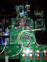
FPGA and CPLD are different in some ways and I recommend to use CPLD for data conversion in DACs. FPGA will work, but CPLD produce less digital noise 😉EPM240 is a CPLD, @miro1360 has been working on a project for the DAC for signal switching between 3 I2S signals (lets say USB, Bluetooth, another 1), in addition it will be eliminating the logic gates as the CPLD will be programmed to work in their place, there are obvious advantages short signal path for one, it'd be much better if one IC can perform the job of 6 or 8 or 10 ICs. I have tried it with AD1865 and TDA1541 yes there is a difference in sound quality.
@miro1360 check this one out:
https://www.aliexpress.com/item/1005003749170513.html?spm=a2g0o.cart.0.0.4ff838da0cfTrY&mp=1
As I have some knowledge of verilog I am considering using this one, you thoughts opinion please.
Signal switching, I2S to PCM, I2C display, and may be an IR and optical encoder option.
So it depends on the complexity ... with FPGA you can do much more work (but is that needed in DAC?).
1. It can have some advantage, you can try that 😉Hi, I am new to this thread, but I have been reading it for a few weeks. Quite interesting developments here 🙂 I started working on the design of AD1865 based DAC and plan to utliize CPLD for I2S/RJ conversion. I intend to implement EPM240 on my PCB. Since I have no deep experience with CPLD I thought I would ask the experts for some advice.
1. Does it make sense to use one of EPM240's global clock pins (GCLK) for I2S BCK signal input? Would this bring any advantage, disadvantage, or is simply irrelevant? BCK would be fastest signal in I2S and as far as I understand the current @miro1360 VHDL code, BCK is driving the RJ conversion.
2. Is the choice I/O banks relevant? I can connect I2S input and RJ output to a single I/O bank, or can use one I/O bank for I2S input and the other I/O bank for RJ output. Both I/O banks are powered with 3.3V.
Thanks in advance.
F
2. It can be only if the other I/O bank is powered from another PSU. It is often used for logic conversion (different voltages, again needs another PSU with different voltage). On the single PSU I am not that sure, I will say no significant advantage 🙂
The first significant factor is the sound (there should be no cracking or similar noises). Second you can check with oscilloscope if the sinewave is constructed from "stairs", you can see that on the scope. You can measure some parameters but it's hard to measure. You can, for example, send individual bits via arduino and measure voltages on DAC output (with some precise I/V resistor connected with AD1862, or a precise I/V circuit). For this measurement you need very precise voltmeter, and even with that you won't measure with complete accuracy in home conditions. You can measure the MSB voltage, and then some combinations down to the lowest accuracy your voltmeter can measure or your I/V can convert (you'll probably end up somewhere around 12-bit, so you won't measure the remaining accuracy or whether if it was damaged during the recycling process). So the best way is to have reference and compare sound .. if you're happy with the sound, then what else? 😊If I would buy the AD1862 by some AE shop, how could I test if they are genuine w/o just guessing based on the print on it? Is there anything one could measure?
PSU2-mini: Is a heat sink required for powering something like the clean side of the I2SoverUSB?
The 'clean' side of things is burning 100mA approx.. I have around 8V raw into the regulator. Luke warm. Hardly enough for me to think about heatsinking.PSU2-mini: Is a heat sink required for powering something like the clean side of the I2SoverUSB?
Ahhh true, i calced xmos into the supply. 100mA can be easily soaked by the pcb plane with few Vin above required.The 'clean' side of things is burning 100mA approx.. I have around 8V raw into the regulator. Luke warm. Hardly enough for me to think about heatsinking.
I had thought that maybe by looking at the spectrum, the THD level and distribution, it could be possible to see if it's a real AD1862.You can measure some parameters but it's hard to measure. You can, for example, send individual bits via arduino and measure voltages on DAC output (with some precise I/V resistor connected with AD1862, or a precise I/V circuit). For this measurement you need very precise voltmeter, and even with that you won't measure with complete accuracy in home conditions.
And for the very end, before the final closing of the box. I tested the U30 USB/I2S card and the Burson V7 Classic opamp. The test is purely subjective, in my audio system. U30 and V7C are there thanks to @Brijac .
U30 USB/I2S:
Excellent sound, a bit brighter and more detailed than the Amanero clone. A little less bass, which therefore seems better defined but also a little sharper treble. As far as the Win drivers for the card is concerned, there is ASIO and WASAPI, but there is no KS (Amenero has KS driver). ASIO sounds a lot better than WASAPI 😳. In principle, Amanero subjectively agrees better with AD1862, more bass and warmth, softer treble. Epilogue - I returned the Amanero clone. I think the U30 would be more suitable for AD1865, PCM1702 or PCM56 than the Amanero clone, but that needs to be checked.
V7 Classic opamp:
Next up is Sparkos SS3601 vs Burson V7 Classic (dual with adapter). In this case, Burson gave a slightly warmer sound and softer highs, without losing details. The sound is somewhat "cheerier" with the V7C. It's just that the DC offset is big, even 20-30mV, but it will be reduced with those trimmers on the opamp. Epilogue - I kept the V7C.
I'm very pleased with how this turned out both sonically and visually. And that's the finale, there are no more tests, this device is finished for a long time. 😁
Attachments
Last edited:
- Home
- Source & Line
- Digital Line Level
- DAC AD1862: Almost THT, I2S input, NOS, R-2R