Can't stand with the temptation with Miro's DAC, one of my friends also completed one board. But he has a strange problem that I am unable to solve and would like to post here to find heros here-:
The problem is when he playing a left-right channel testing track, it seems that is okay with left channel when test left, but when testing right channel, both left and righ speakers sound. And
When playing the polarity test, only right speaker sound when playing in-phase and only left speaker sound when playing out-of-the-phase.
do you know what the possible problem is?
Thank
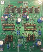
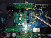
As always, pictures showing details of how things are connected will help the members here to scrutinize for errors.

He said he got the 4.7k resistor on JLsound board and removed the op-amp for making the photo clearer.

Hm, looks not very clean. C7 needs pin resoldering.
The yellow and red wires are from an external PSU? The picture shows like a short between them, maybe it is only visual overlap 🤔
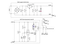
Problem can be in jlsounds configuration.
... make sure he installed J4 jumper on the jlsounds board (only this one)
... make sure the 4.7k resistor on JLsound board is installed correctly (normally it is located on DAC PCB, R13)
The yellow and red wires are from an external PSU? The picture shows like a short between them, maybe it is only visual overlap 🤔
Problem can be in jlsounds configuration.
... make sure he installed J4 jumper on the jlsounds board (only this one)
... make sure the 4.7k resistor on JLsound board is installed correctly (normally it is located on DAC PCB, R13)
Is the JLSounds board the latest FIO version?He said he got the 4.7k resistor on JLsound board and removed the op-amp for making the photo clearer.
View attachment 1239897
Not only that, I see a lot of cold solders.Hm, looks not very clean. C7 needs pin resoldering.
They are not good for sure, the soldering iron was not heated enough, it did not pull the solder into the metallized hole. Or the solder wire is bad, not enough flux. Everything needs to be re-soldered properly. Apply flux to all joints and solder again. As it is, it will only cause problems.
I have another question on hooking up JLSounds I2S while bypassing shift registers. After cutting JP1/JP2 am I right in assuming that I can use the points labeled DR and DL to tie in the DR and DL from JLSounds ? I can't tell if they tie into the traces from JP1/JP2 to the DAC by looking at the board.
Many thanks
Many thanks
Attachments
Yes. If you can't tell visually, use a multimeter to measure for short before you cut Jp1/Jp2. You should get a short
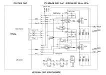
Miro, I made a slightly different I/V circuit for your DACs. It is made as a modular assembly. Both OPAs are removed from the DAC board, transferred to a new PCB and the connectors are inserted into the bases of the OPAs on the Miro DAC board. If it doesn't work, it takes 5 minutes to get everything back to its previous state. Due to the higher current, larger heatsinks are needed on the PSU2 (+-12V). I put 80mA of quiescent current through the mosfets, and it can be more or less. I also envisioned the possibility of using single or dual OPAs.
.
Along the way, I also made a small Mute timer, because this circuit outputs about 3VDC when it is turned off. It doesn't last long, but it can be harmful to other devices. The OPA without a mosfet gives about 1.8VDC at the outputs for about 15-20s, so Mute is definitely useful.
Thanks to the mosfet source follower large gate resistance and VGS, any OPA is forced to work always in A class, and as single ended up to about 2.5VRMS.
Tested with AD1860 and OPA2604/OPA1612. I'll put in better components later when I'm sure everything is working as it should. I finished late last night, just to check if it works. About sound impressions later.
I also added some connectors that allow me to try this circuit with a Pavouk DAC or another DAC with Iout. For that I need an external supply +-12V, I don't know if it will ever be tried.
Attachments

Last edited:
Little time was found for AD1862. The rehearsal is only next weekend. The electrolytic capacitors are all Elna Silmic, except for 4x47uF on the power supply of the digital part of the AD chip, I put a Panasonic FR there.
In the meantime, I didn't have time to test that I/V assembly with IRF510 in more detail. So far, the first impressions are that the sound is fuller, with more bass and the middle and highs are a little softer. That's all with AD1860 and PCM56 for the first test. It doesn't help that there are a lot of wires and connectors, I could overcome that only with a new PCB for the DAC. If that circuit remains, I will wire it from the bottom directly to the DAC board. I can't do that for testing, because I'm going to change DAC boards.
In the meantime, I didn't have time to test that I/V assembly with IRF510 in more detail. So far, the first impressions are that the sound is fuller, with more bass and the middle and highs are a little softer. That's all with AD1860 and PCM56 for the first test. It doesn't help that there are a lot of wires and connectors, I could overcome that only with a new PCB for the DAC. If that circuit remains, I will wire it from the bottom directly to the DAC board. I can't do that for testing, because I'm going to change DAC boards.
Attachments
Last edited:
By the way, if anyone is interested, the PCM56P-K that I bought on ebay from the seller Polida work, and they work great right out of the bag. If that new I/V circuit of mine doesn't kill them, they'll probably work forever. 🙂
https://www.ebay.com/itm/362255965846
https://www.ebay.com/itm/362255965846
- Home
- Source & Line
- Digital Line Level
- DAC AD1862: Almost THT, I2S input, NOS, R-2R